LP3972 www.ti.
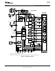
LP3972 SNVS468K – SEPTEMBER 2006 – REVISED MAY 2013 www.ti.com Application Circuits Back-up Battery VIN + - LDO1 BUCK1 LDO2 LDO3 BUCK2 LP3972 LDO4 LDO5 BUCK3 SYNC SCL SDA GPIO2 GPIO1/nCHG_EN EXT_WAKEUP SPARE PWR_EN PWR_ON nTEST_JIG nRSTI SYS_EN nRSTO nBATT_FLT RTC Figure 1.
LP3972 www.ti.com SNVS468K – SEPTEMBER 2006 – REVISED MAY 2013 Li-ion/polymer cell 14 31 20 Vin_BUCK1 26 Vin_BUCK2 VDDA 27 6 Vin_BUCK3 VIN DC SOURCE 4.5 ± 5.5V VinLDO4 Cvdd 4.7 PF VinLDO5 See notes + LP3972 PMIC SYNC 40 Cchg_det 4.7 PF APPLICATION PROCESSOR 35 Clock divider 37 PWR_EN Lsw1 2.2 PH COMP 39 EOC CPU CORE SW1 BUCK1 10 PF VFB1 5 VinBUBATT 15 Lsw2 2.
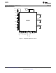
LP3972 SNVS468K – SEPTEMBER 2006 – REVISED MAY 2013 www.ti.com Connection Diagram 30 29 28 27 26 25 24 23 22 21 21 22 23 24 25 26 27 28 29 30 31 20 20 31 32 19 19 32 33 33 18 18 34 17 17 34 35 16 16 35 36 15 15 36 37 14 14 37 38 13 13 38 39 12 12 39 40 11 11 40 1 2 3 4 5 6 7 8 9 10 10 9 8 Top View 7 6 5 4 3 2 1 Bottom View Note: Circle marks pin 1 position. 40-Pin WQFN, Package Number RSB0040A PIN DESCRIPTIONS Pin No.
LP3972 www.ti.com SNVS468K – SEPTEMBER 2006 – REVISED MAY 2013 PIN DESCRIPTIONS (continued) Pin No. Name I/O Type (1) 20 VIN Buck2 I PWR 21 SDA I/O D I2C Data (Bidirectional) 22 SCL I D I2C Clock 23 FB2 I A Buck2 input feedback terminal 24 nRSTO O D Reset output from the PMIC to the processor 25 VOUT LDO5 O PWR LDO5 output 26 VIN LDO5 I PWR Power input to LDO5, this can be connected to VIN or to a separate 1.8V supply.
LP3972 SNVS468K – SEPTEMBER 2006 – REVISED MAY 2013 www.ti.com Operating Ratings VIN 2.7V to 5.5V VINLDO4, 5 1.74 to VIN −40°C to +125°C Junction Temperature (TJ) −40°C to +85°C Operating Temperature (TA) Maximum Power Dissipation (TA = 70°C) (1) (2) (1) (2) 2.2W In applications where high power dissipation and/or poor package thermal resistance is present, the maximum ambient temperature may have to be derated.
LP3972 www.ti.com SNVS468K – SEPTEMBER 2006 – REVISED MAY 2013 Default Voltage Option (1) (2) (3) Version LP3972SQ-A514 Enable Version A LDO_RTC LP3972SQ-A413 Version A — 2.8 — 2.8 LDO1 SYS_EN 1.8 SYS_EN 1.8 LDO2 SYS_EN 1.8D SYS_EN 1.8D LDO3 SYS_EN 3D SYS_EN 3D LDO4 SYS_EN 3D SYS_EN 2.8D LDO5 PWR_EN 1.4 PWR_EN 1.4 BUCK1 PWR_EN 1.4 PWR_EN 1.4 BUCK2 SYS_EN 3.3 SYS_EN 3 BUCK3 SYS_EN 1.8 SYS_EN Version LP3972SQ-E514 Enable LDO_RTC 1.
LP3972 SNVS468K – SEPTEMBER 2006 – REVISED MAY 2013 www.ti.com LDO RTC Unless otherwise noted, VIN = 3.6V, CIN = 1.0 µF, COUT = 0.47 µF, COUT (VRTC) = 1.0 µF ceramic. Typical values and limits appearing in normal type apply for TJ = 25°C. Limits appearing in boldface type apply over the entire junction temperature range for operation, −40°C to +125°C (1) (2) (3) (4) Symbol Parameter Test Conditions Min Typ Max 2.632 2.8 2.968 V VIN = (VOUT nom + 1.0V) to 5.5V (5) Load Current = 1 mA 0.
LP3972 www.ti.com SNVS468K – SEPTEMBER 2006 – REVISED MAY 2013 LDOs 1 to 5 Unless otherwise noted, VIN = 3.6V, CIN = 1.0 µF, COUT = 0.47 µF, COUT (VRTC) = 1.0 µF ceramic. Typical values and limits appearing in normal type apply for TJ = 25°C. Limits appearing in boldface type apply over the entire junction temperature range for operation, −40°C to +125°C (1) (2) (3) (4) (5) (6) (7) Symbol Parameter Test Conditions Max Unit 3 % VIN =3.1V to 5.0V (5), Load Current = 1 mA 0.
LP3972 SNVS468K – SEPTEMBER 2006 – REVISED MAY 2013 www.ti.com LDO Dropout Voltage vs. Load Current Collect Data For All LDOs Dropout Voltage vs. Load Current Change in Output Voltage vs. Load Current 200 CHANGE IN OUTPUT VOLTAGE (mV) DROPOUT VOLTAGE (mV) 300 250 200 150 100 REG1 3.3V OUTPUT 50 0 0 200 400 600 800 150 100 REG1 3.3V OUTPUT REG3 1.3V OUTPUT 0 -50 VIN = 3.6V -100 1000 1200 REG2 2.5V OUTPUT 50 LOAD CURRENT (mA) 0 200 400 600 800 1000 1200 LOAD CURRENT (mA) Figure 3.
LP3972 www.ti.com SNVS468K – SEPTEMBER 2006 – REVISED MAY 2013 Buck Converters SW1, SW2, SW3 Unless otherwise noted, VIN = 3.6V, CIN = 10 µF, COUT = 10 µF, LOUT = 2.2 µH ceramic. Typical values and limits appearing in normal type apply for TJ = 25°C.
LP3972 SNVS468K – SEPTEMBER 2006 – REVISED MAY 2013 www.ti.com Line Transient Response VIN = 3 – 3.6 V, VOUT = 1.2 V, 250 mA load VIN = 3, 3.5 volts VOUT = 1.4 volts Forced PWM 90.00 VIN = 5.5V EFFICIENCY (%) 72.00 VIN = 5V 54.00 36.00 18.00 0.00 1 1e1 1e2 1e3 4.03 Ps 1e4 OUTPUT CURRENT (mA) Figure 10. Figure 11. Mode Change Load transients 20 mA to 560 mA VOUT = 1.4 volts [PFM to PWM] VIN = 4.1 volts Load Transient 3.6 VIN, 3.3 VOUT, 0 – 100 mA load 4.03 Ps 4.0 Ps Figure 12. Figure 13.
LP3972 www.ti.com SNVS468K – SEPTEMBER 2006 – REVISED MAY 2013 Back-Up Charger Electrical Characteristics Unless otherwise noted, VIN = VBATT = 3.6V. Typical values and limits appearing in normal type apply for TJ = 25°C. Limits appearing in boldface type apply over the entire junction temperature range for operation, −40°C to +125°C (1) (2) (3) Symbol Parameter Test Conditions VIN Operational Voltage Range Voltage at VIN IOUT Backup Battery Charging Current VIN = 3.6V, Backup_Bat = 2.
LP3972 SNVS468K – SEPTEMBER 2006 – REVISED MAY 2013 www.ti.com Logic Inputs and Outputs DC Operating Conditions (1) Logic Inputs (SYS_EN, PWR_EN, SYNC, nRSTI, PWR_ON, nTEST_JIG, SPARE and GPI's) Symbol Parameter VIL Low Level Input Voltage VIH High Level Input Voltage ILEAK Input Leakage Current (1) Test Conditions Min Max Unit 0.5 V −1 +1 µA Min Max Unit 0.5 V +5 µA VRTC − 0.5V V All voltages are with respect to the potential at the GND pin.
LP3972 www.ti.com SNVS468K – SEPTEMBER 2006 – REVISED MAY 2013 Detailed Description Buck Converter Operation DEVICE INFORMATION The LP3972 includes three high efficiency step down DC-DC switching buck converters. Using a voltage mode architecture with synchronous rectification, the buck converters have the ability to deliver up to 1600 mA depending on the input voltage, output voltage, ambient temperature and the inductor chosen.
LP3972 SNVS468K – SEPTEMBER 2006 – REVISED MAY 2013 www.ti.com VSW 2V/DIV IL 200 mA/DIV VIN = 3.6V VOUT = 1.5V IOUT = 400 mA VOUT 10 mV/DIV AC Coupled TIME (200 ns/DIV) Figure 15. Typical PWM Operation Internal Synchronous Rectification While in PWM mode, the converters uses an internal NFET as a synchronous rectifier to reduce rectifier forward voltage drop and associated power loss.
LP3972 www.ti.com SNVS468K – SEPTEMBER 2006 – REVISED MAY 2013 During PFM operation, the converter positions the output voltage slightly higher than the nominal output voltage during PWM operation, allowing additional headroom for voltage drop during a load transient from light to heavy load. The PFM comparators sense the output voltage via the feedback pin and control the switching of the output FETs such that the output voltage ramps between <0.6% and <1.7% above the nominal PWM output voltage.
LP3972 SNVS468K – SEPTEMBER 2006 – REVISED MAY 2013 www.ti.com LDO - LOW DROP OUT OPERATION The LP3972 can operate at 100% duty cycle (no switching; PMOS switch completely on) for low drop out support of the output voltage. In this way the output voltage will be controlled down to the lowest possible input voltage. When the device operates near 100% duty cycle, output voltage ripple is approximately 25 mV.
LP3972 www.ti.com SNVS468K – SEPTEMBER 2006 – REVISED MAY 2013 I2C Compatible Interface I2C DATA VALIDITY The data on SDA line must be stable during the HIGH period of the clock signal (SCL). In other words, state of the data line can only be changed when CLK is LOW. SCL SDA data valid data change allowed data change allowed data change allowed data valid Figure 19. I2C START and STOP CONDITIONS START and STOP bits classify the beginning and the end of the I2C session.
LP3972 SNVS468K – SEPTEMBER 2006 – REVISED MAY 2013 www.ti.com Write Cycle start msb Chip Address lsb w ack Msb Register Add lsb ack msb DATA lsb ack stop w ack addr = 02h ack DGGUHVV K¶02 data ack stop SCL SDA start Id = 34h Figure 21. Write cycle Read Cycle When a READ function is to be accomplished, a WRITE function must precede the READ function as follows.
LP3972 www.ti.com SNVS468K – SEPTEMBER 2006 – REVISED MAY 2013 MULTI-BYTE I2C COMMAND SEQUENCE To correctly function with the Monahan’s Power Management I2C the LP3972’s I2C serial interface shall support Random register Multi-byte command sequencing: During a multi-byte write the Master sends the Start command followed by the Device address, which is sent only once, followed by the 8 Bit register address, then 8 bits of data.
LP3972 SNVS468K – SEPTEMBER 2006 – REVISED MAY 2013 www.ti.
LP3972 www.ti.com SNVS468K – SEPTEMBER 2006 – REVISED MAY 2013 System Control Register (SCR) 8h’07 Definitions Bit Access Name 7-1 — — 0 R/W CLK_SCL Description Reserved External Clock Select 0 = Internal Oscillator clock for Buck Converters 1 = External 13 MHz Oscillator clock for Buck Converters OUTPUT VOLTAGE ENABLE REGISTER 1 This register enables or disables the low voltage supplies LDO1 and Buck1. See details below.
LP3972 SNVS468K – SEPTEMBER 2006 – REVISED MAY 2013 www.ti.com OUTPUT VOLTAGE ENABLE REGISTER 2 This 8 bit output register enables and disables the output voltages on the LDOs 2,3,4 supplies.
LP3972 www.ti.
LP3972 SNVS468K – SEPTEMBER 2006 – REVISED MAY 2013 www.ti.
LP3972 www.ti.com SNVS468K – SEPTEMBER 2006 – REVISED MAY 2013 VCC_COMM TARGET VOLTAGE 1 DUMMY REGISTER (CDTV1) VCC_COMM Target Voltage 1 Dummy Register (CDTV1) 8h’26 Write Only (1) Bit 7 6 Designation Reset Value (1) 5 4 3 2 Reserved 0 1 0 0 0 0 2 1 0 0 0 1* (1) 0 (1) Output Voltage 0 0 0 0 CDTV1 must be writable by an I2C controller.
LP3972 SNVS468K – SEPTEMBER 2006 – REVISED MAY 2013 www.ti.
LP3972 www.ti.com SNVS468K – SEPTEMBER 2006 – REVISED MAY 2013 LDO1 (VCC_MVT) TARGET VOLTAGE 2 REGISTER LDO1 (VCC_MVT) Target Voltage 2 Register (MDTV2) 8h’33 Bit 7 6 Designation Reset Value 5 4 3 Reserved 0 2 1 0 1 1 Output Voltage (OV) 0 0 0 1 0 LDO1 (VCC_MVT) Target Voltage 2 Register (MDTV2) 8h’33 Definitions Bit Access Name 7:5 — — 4:0 R/W L1OV Description Reserved Data Code 5h’0 5h’1 5h’2 5h’3 5h’4 5h’5 5h’6 5h’7 5h’8 5h’9 5h’A 5h’B 5h’C 5h’D-5h’F Output Voltage 1.700 1.
LP3972 SNVS468K – SEPTEMBER 2006 – REVISED MAY 2013 www.ti.
LP3972 www.ti.
LP3972 SNVS468K – SEPTEMBER 2006 – REVISED MAY 2013 www.ti.
LP3972 www.ti.
LP3972 SNVS468K – SEPTEMBER 2006 – REVISED MAY 2013 www.ti.
LP3972 www.ti.
LP3972 SNVS468K – SEPTEMBER 2006 – REVISED MAY 2013 www.ti.com Bit Access Name 1 R WUPT TEST_JIG Pin Wake Up Status 0 = No wake up event 1 = Wake up event Description 0 R WUPS SPARE Pin Wake Up Status 0 = No wake up event 1 = Wake up event BACKUP BATTERY CHARGER CONTROL REGISTER (BCCR) This register specifies the status of the main battery supply.
LP3972 www.ti.com SNVS468K – SEPTEMBER 2006 – REVISED MAY 2013 MARVELL PXA INTERNAL 2 REVISION REGISTER (II2RR) 8H’8F Bit 7 6 5 4 0 0 0 0 Designation Reset Value 3 2 1 0 0 0 0 0 II2RR MARVELL PXA INTERNAL 2 REVISION REGISTER (II2RR) 8H’8F DEFINITIONS Bit Access Name 7:0 R II2RR Description Intel internal usage register for revision information.
LP3972 SNVS468K – SEPTEMBER 2006 – REVISED MAY 2013 www.ti.com Example 2) Voltage change Sequence PMIC Register Address PMIC Register Name Register Data Description 8h’24 ADTV2 00010111 Sets the VCC_APPS target voltage 2 to 1.3 V 8h’2A SDTV2 00001111 Sets the VCC_SRAM target voltage 2 to 1.1 V 8h’20 VCC1 00110011 Enable VCC_SRAM and VCC_APPS to change to their programmed target values.
LP3972 www.ti.com SNVS468K – SEPTEMBER 2006 – REVISED MAY 2013 POWER DOMAIN ENABLES PMU Output HW Enable SW Enable LDO_RTC — — LDO1 (VCC_MVT) SYS_EN LDO1_EN LDO2 SYS_EN LDO2_EN LDO3 SYS_EN LDO3_EN LDO4 SYS_EN LDO4_EN LDO5 (VCC_SRAM) PWR_EN S_EN Buck1 (VCC_APPS) PWR_EN A_EN BUCK2 SYS_EN B2_EN BUCK3 SYS_EN B3_EN POWER DOMAINS SEQUENCING (DELAY) By default SYS_EN must be on to have PWR_EN enable but this feature can be switched off by register bit BP_SYS.
LP3972 SNVS468K – SEPTEMBER 2006 – REVISED MAY 2013 www.ti.com PWR_ON nTEST_JIG SPARE OR EXT_WAKEUP PWR_ON EXT_WAKEUP nTEST_JIG 10 ms SPARE Internal Thermal Early Warning Figure 28. WAKEUP register bits Reason for WAKEUP WUP0 SPARE WUP1 TEST_JIG WUP2 PWR_ON short pulse WUP3 PWR_ON long pulse TSD_EW TSD Early Warning INTERNAL THERMAL SHUTDOWN PROCEDURE Thermal shutdown is build to generate early warning (typ. 125°C) which triggers the EXT_WAKEUP for the processor acknowledge.
LP3972 www.ti.
LP3972 SNVS468K – SEPTEMBER 2006 – REVISED MAY 2013 www.ti.com 1) Thermal warning flag @ Temp ~ > ~125oC is issued at the wakeup port: ~30oC hysteresis Temp 125oC Warning flag 2) Binary coded thermal management flags in status registers, bct<2:0>: flag6 flag5 flag4 flag3 flag2 flag1 cool 17oC 20oC 43oC 46oC 62oC 65oC 83oC 86oC 106oC 108oC 128oC 130oC Temp Figure 29. Application Note - LP3972 Reset Sequence INITIAL COLD START POWER ON SEQUENCE 1.
LP3972 www.ti.com SNVS468K – SEPTEMBER 2006 – REVISED MAY 2013 t3 t1 t4 VIN BU Batt 1. VCC_RTC 2. nRSTO VIN Main Batt 3,4. nBATT_FLT SYS_EN 5. PXA27x Output 6. High-Volt_PD PWR_EN 7. PXA27x Output 8. Low-Volt_PD t2 nRESET_OUT PXA27x Output 13 MHZ_OSC PXA27x Output t5 9,10. * Note that BOTH nRSTO and nBATT_FLT need to be de-asserted before SYS_EN is enabled. The sequence of the two signals is independent of each other and can occur is either order. Figure 30.
LP3972 SNVS468K – SEPTEMBER 2006 – REVISED MAY 2013 www.ti.com 8. The Applications processor asserts PWR_EN, the LP3972 enables the low-voltage regulators. 9. Countdown timer expires; If enabled power domains are OK (I2C read) the power up sequence continues by enabling the processors 13 MHz oscillator and PLL’s. 10. The Applications processor begins the execution of code. APPLICATION HINTS LDO CONSIDERATIONS External Capacitors The LP3972’s regulators require external capacitors for regulator stability.
LP3972 www.ti.com SNVS468K – SEPTEMBER 2006 – REVISED MAY 2013 CAP VALUE (% OF NOMINAL 1 PF) performance figures in general. As an example, Figure 31 shows a typical graph comparing different capacitor case sizes in a Capacitance vs. DC Bias plot. As shown in the graph, increasing the DC Bias condition can result in the capacitance value falling below the minimum value given in the recommended capacitor specifications table.
LP3972 SNVS468K – SEPTEMBER 2006 – REVISED MAY 2013 www.ti.com ISAT > IOUTMAX + IRIPPLE * § VOUT ¨ ¨ VIN © § ¨ ¨ © § ¨ ¨ © § VIN - VOUT ¨ ¨ 2* L © * §1 ¨ ¨f © § ¨ ¨ © where IRIPPLE = where • • • • • • IRIPPLE: Average to peak inductor current IOUTMAX: Maximum load current (1500 mA) VIN: Maximum input voltage in application L: Min inductor value including worst case tolerances (30% drop can be considered for method 1) f: Minimum switching frequency (1.
LP3972 www.ti.com SNVS468K – SEPTEMBER 2006 – REVISED MAY 2013 The output voltage ripple is caused by the charging and discharging of the output capacitor and also due to its ESR and can be calculated as: IRIPPLE VPP-C = 4 * f *C (4) Voltage peak-to-peak ripple due to ESR can be expressed as follows VPP-ESR = (2 * IRIPPLE) * RESR (5) Because these two components are out of phase the RMS value can be used to get an approximate value of peak-to-peak ripple.
LP3972 SNVS468K – SEPTEMBER 2006 – REVISED MAY 2013 www.ti.com Board Layout Considerations PC board layout is an important part of DC-DC converter design. Poor board layout can disrupt the performance of a DC-DC converter and surrounding circuitry by contributing to EMI, ground bounce, and resistive voltage loss in the traces. These can send erroneous signals to the DC-DC converter IC, resulting in poor regulation or instability.
LP3972 www.ti.com SNVS468K – SEPTEMBER 2006 – REVISED MAY 2013 REVISION HISTORY Changes from Revision J (May 2013) to Revision K • Page Changed layout of National Data Sheet to TI format ..........................................................................................................
PACKAGE OPTION ADDENDUM www.ti.
PACKAGE OPTION ADDENDUM www.ti.
PACKAGE OPTION ADDENDUM www.ti.com 1-Nov-2013 In no event shall TI's liability arising out of such information exceed the total purchase price of the TI part(s) at issue in this document sold by TI to Customer on an annual basis.
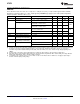
PACKAGE MATERIALS INFORMATION www.ti.com 11-Oct-2013 TAPE AND REEL INFORMATION *All dimensions are nominal Device Package Package Pins Type Drawing SPQ Reel Reel A0 Diameter Width (mm) (mm) W1 (mm) B0 (mm) K0 (mm) P1 (mm) W Pin1 (mm) Quadrant LP3972SQ-0514/NOPB WQFN RSB 40 1000 178.0 12.4 5.3 5.3 1.3 8.0 12.0 Q1 LP3972SQ-5810/NOPB WQFN RSB 40 1000 178.0 12.4 5.3 5.3 1.3 8.0 12.0 Q1 LP3972SQ-A413/NOPB WQFN RSB 40 1000 178.0 12.4 5.3 5.3 1.3 8.0 12.
PACKAGE MATERIALS INFORMATION www.ti.com 11-Oct-2013 Device LP3972SQX-I514/NOPB Package Package Pins Type Drawing WQFN RSB 40 SPQ Reel Reel A0 Diameter Width (mm) (mm) W1 (mm) 4500 330.0 12.4 5.3 B0 (mm) K0 (mm) P1 (mm) 5.3 1.3 8.0 W Pin1 (mm) Quadrant 12.0 Q1 *All dimensions are nominal Device Package Type Package Drawing Pins SPQ Length (mm) Width (mm) Height (mm) LP3972SQ-0514/NOPB WQFN RSB 40 1000 210.0 185.0 35.0 LP3972SQ-5810/NOPB WQFN RSB 40 1000 210.0 185.
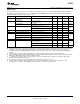
PACKAGE MATERIALS INFORMATION www.ti.com 11-Oct-2013 Device Package Type Package Drawing Pins SPQ Length (mm) Width (mm) Height (mm) LP3972SQX-E514/NOPB WQFN RSB 40 4500 367.0 367.0 35.0 LP3972SQX-I414/NOPB WQFN RSB 40 4500 367.0 367.0 35.0 LP3972SQX-I514/NOPB WQFN RSB 40 4500 367.0 367.0 35.
MECHANICAL DATA RSB0040A SQF40A (Rev B) www.ti.
IMPORTANT NOTICE Texas Instruments Incorporated and its subsidiaries (TI) reserve the right to make corrections, enhancements, improvements and other changes to its semiconductor products and services per JESD46, latest issue, and to discontinue any product or service per JESD48, latest issue. Buyers should obtain the latest relevant information before placing orders and should verify that such information is current and complete.