
Datasheet
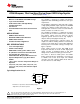

1PF
BYPASS
LP3985
V
IN
V
OUT
V
EN
3(A1)
5(C1)
4(A3)
2(B2)
1PF
1(C3)
*
LP3985
www.ti.com
SNVS087AC –OCTOBER 2000–REVISED MAY 2013
LP3985 Micropower, 150mA Low-Noise Ultra Low-Dropout CMOS Voltage Regulator
Check for Samples: LP3985
1
FEATURES
DESCRIPTION
The LP3985 is designed for portable and wireless
2
• Miniature 5-I/O DSBGA and USON Package
applications with demanding performance and space
• Logic Controlled Enable
requirements.
• Stable with Ceramic and High Quality
The LP3985 is stable with a small 1µF ±30% ceramic
Tantalum Capacitors
or high-quality tantalum output capacitor. The DSBGA
• Fast Turn-on
requires the smallest possible PC board area - the
total application circuit area can be less than 2.0mm x
• Thermal Shutdown and Short-Circuit Current
2.5mm, a fraction of a 1206 case size.
Limit
The LP3985's performance is optimized for battery
APPLICATIONS
powered systems to deliver ultra low noise, extremely
low dropout voltage and low quiescent current.
• CDMA Cellular Handsets
Regulator ground current increases only slightly in
• Wideband CDMA Cellular Handsets
dropout, further prolonging the battery life.
• GSM Cellular Handsets
An optional external bypass capacitor reduces the
• Portable Information Appliances
output noise without slowing down the load transient
response. Fast startup time is achieved by utilizing an
KEY SPECIFICATIONS
internal power-on circuit that actively pre-charges the
bypass capacitor.
• 2.5 to 6.0V Input Range
Power supply rejection is better than 50dB at low
• 150mA Verified Output
frequencies and starts to roll off at 1kHz. High power
• 50dB PSRR at 1kHz @ VIN = VOUT + 0.2V
supply rejection is maintained down to low input
• ≤1.5μA Quiescent Current when Shut Down
voltage levels common to battery operated circuits.
• Fast Turn-On time: 200μs (typ.)
The device is ideal for mobile phone and similar
• 100mV Maximum Dropout with 150mA Load
battery powered wireless applications. It provides up
to 150mA, from a 2.5V to 6V input. The LP3985
• 30μVrms Output Noise (typ.) Over 10Hz to
consumes less than 1.5µA in disable mode and has
100kHz
fast turn-on time less than 200µs.
• −40 to +125°C Junction Temperature Range for
Operation
• 2.5V, 2.6V, 2.7V, 2.8V, 2.85V, 2.9V, 3.0V, 3.1V,
3.2V, 3.3V, 4.7V, 4.75V, 4.8V and 5.0V outputs
standard
Typical Application Circuit
Pin Numbers in parenthesis indicate DSBGA package.
* Optional Noise Reduction Capacitor.
Figure 1.
1
Please be aware that an important notice concerning availability, standard warranty, and use in critical applications of
Texas Instruments semiconductor products and disclaimers thereto appears at the end of this data sheet.
2All trademarks are the property of their respective owners.
PRODUCTION DATA information is current as of publication date.
Copyright © 2000–2013, Texas Instruments Incorporated
Products conform to specifications per the terms of the Texas
Instruments standard warranty. Production processing does not
necessarily include testing of all parameters.