
Datasheet

LP3990
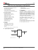
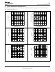
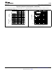
V
OUT
V
IN
1.0 PF
1.0 PF
V
EN
GND
V
IN
V
EN
6
5
2
1
V
OUT
(WQFN pin connections shown)
LP3990
SNVS251I –MAY 2004–REVISED MAY 2013
LP3990 150-mA Linear Voltage Regulator for Digital Applications
1 Features 4 Applications
1
• 1% Voltage Accuracy at Room Temperature
• Cellular Handsets
• Stable with Ceramic Capacitor • Hand-Held Information Appliances
• Logic Controlled Enable
5 Description
• No Noise Bypass Capacitor Required
The LP3990 regulator is designed to meet the
• Thermal-Overload and Short-Circuit Protection
requirements of portable, battery-powered systems
providing an accurate output voltage, low noise, and
2 Key Specifications
low quiescent current. The LP3990 will provide a 0.8-
V output from the low input voltage of 2 V at up to
• Input Voltage Range, 2.0 to 6.0 V
150-mA load current. When switched into shutdown
• Output Voltage Range, 0.8 to 3.3 V
mode via a logic signal at the enable pin, the power
• Output Current, 150 mA
consumption is reduced to virtually zero.
• Output Stable - Capacitors, 1.0 µF
The LP3990 is designed to be stable with space
• Virtually Zero I
Q
(Disabled), <10 nA
saving ceramic capacitors as small as 1.0 µF.
• Very Low I
Q
(Enabled), 43 µA
Performance is specified for a -40°C to 125°C
• Low Output Noise, 150 µV
RMS junction temperature range.
• PSRR, 55 dB at 1 kHz
For output voltages other than 0.8 V, 1.2 V, 1.35 V,
• Fast Start-up, 105 µs
1.5 V, 1.8 V, 2.5 V, 2.8 V, or 3.3 V, please contact
the Texas Instruments sales office.
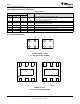
3 Package
All available in Lead-Free option:
• 4-bump DSBGA, 1 mm x 1.3 mm
• 6-pin WQFN (SOT-23 Footprint)
• SOT-23
For other package options contact your Texas Instruments sales office.
5.1 Typical Application Circuit
1
An IMPORTANT NOTICE at the end of this data sheet addresses availability, warranty, changes, use in safety-critical applications,
intellectual property matters and other important disclaimers. PRODUCTION DATA.