
Datasheet
LT1054
SWITCHED-CAPACITOR VOLTAGE CONVERTERS
WITH REGULATORS
SLVS033F − FEBRUARY 1990 − REVISED NOVEMBER 2004
1
POST OFFICE BOX 655303 • DALLAS, TEXAS 75265
D Output Current . . . 100 mA
D Low Loss . . . 1.1 V at 100 mA
D Operating Range ...3.5 V to 15 V
D Reference and Error Amplifier for
Regulation
D External Shutdown
D External Oscillator Synchronization
D Devices Can Be Paralleled
D Pin-to-Pin Compatible With the
LTC1044/7660
description/ordering information
The LT1054 is a bipolar, switched-capacitor
voltage converter with regulator. It provides higher
output current and significantly lower voltage
losses than previously available converters. An
adaptive-switch drive scheme optimizes
efficiency over a wide range of output currents.
Total voltage drop at 100-mA output current
typically is 1.1 V. This applies to the full
supply-voltage range of 3.5 V to 15 V. Quiescent
current typically is 2.5 mA.
The LT1054 also provides regulation, a feature previously not available in switched-capacitor voltage
converters. By adding an external resistive divider, a regulated output can be obtained. This output is regulated
against changes in both input voltage and output current. The LT1054 also can be shut down by grounding the
feedback terminal. Supply current in shutdown typically is 100 μA.
The internal oscillator of the LT1054 runs at a nominal frequency of 25 kHz. The oscillator terminal can be used
to adjust the switching frequency or to externally synchronize the LT1054.
The LT1054C is characterized for operation over a free-air temperature range of 0°C to 70°C. The LT1054I is
characterized for operation over a free-air temperature range of −40°C to 85°C.
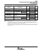
ORDERING INFORMATION
T
A
PACKAGE
†
ORDERABLE
PART NUMBER
TOP-SIDE
MARKING
PDIP (P) Tube of 50 LT1054IP LT1054IP
−40°C to 85°C
SOIC (DW)
Tube of 40 LT1054IDW
LT1054I
40 C
to
85 C
SOIC (DW)
Reel of 2000 LT1054IDWR
LT1054I
PDIP (P) Tube of 50 LT1054CP LT1054CP
0°C to 70°C
SOIC (DW)
Tube of 40 LT1054CDW
LT1054C
SOIC (DW)
Reel of 2000 LT1054CDWR
LT1054C
†
Package drawings, standard packing quantities, thermal data, symbolization, and PCB design guidelines are
available at www.ti.com/sc/package.
Copyright © 2004, Texas Instruments Incorporated
PRODUCTION DATA information is current as of publication date.
Products conform to specifications per the terms of Texas Instruments
standard warranty. Production processing does not necessarily include
testing of all parameters.
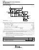
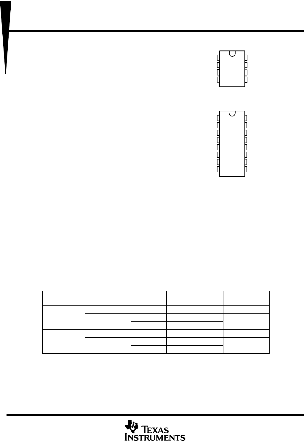
DW PACKAGE
(TOP VIEW)
P PACKAGE
(TOP VIEW)
1
2
3
4
8
7
6
5
FB/SD
CAP+
GND
CAP−
V
CC
OSC
V
REF
V
OUT
1
2
3
4
5
6
7
8
16
15
14
13
12
11
10
9
NC
NC
FB/SD
CAP+
GND
CAP−
NC
NC
NC
NC
V
CC
OSC
V
REF
V
OUT
NC
NC
NC − No internal connection