! ! User’s Guide April 2003 SBAU086
IMPORTANT NOTICE Texas Instruments Incorporated and its subsidiaries (TI) reserve the right to make corrections, modifications, enhancements, improvements, and other changes to its products and services at any time and to discontinue any product or service without notice. Customers should obtain the latest relevant information before placing orders and should verify that such information is current and complete.
EVM IMPORTANT NOTICE Texas Instruments (TI) provides the enclosed product(s) under the following conditions: This evaluation kit being sold by TI is intended for use for ENGINEERING DEVELOPMENT OR EVALUATION PURPOSES ONLY and is not considered by TI to be fit for commercial use.
EVM WARNINGS AND RESTRICTIONS It is important to operate this EVM within the specified input and output ranges described in the EVM User’s Guide. Exceeding the specified input range may cause unexpected operation and/or irreversible damage to the EVM. If there are questions concerning the input range, please contact a TI field representative prior to connecting the input power.
Contents Preface About This Manual This users guide describes the function and operation of the MSC1211EVM. This manual will help you quickly set up the evaluation module and its accompanying software, so that you can rapidly test and evaluate the MSC1211. A complete circuit description, as well as schematic diagram and bill of materials, is included. How to Use This Manual This manual begins with an introductory chapter which describes the EVM and what it can do.
Contents Related Documentation From Texas Instruments Data Sheets: Literature Number: MSC1211 SBAS267 REG1117–5.0,–3.3 SBVS001 ADS8325 SBAS226 MAX3243CPWR SLLS350 TPS3837L30DBVT,TPS3838L30DBVT SLVS292 SN74HC573ADW SCLS147 SN74AC10PWR SCAS529 SN74AHC1G08DBVR SCLS3141 SN74AHC138PWR SCLS2581 FCC Warning This equipment is intended for use in a laboratory test environment only.
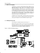
Contents 1 Introduction . . . . . . . . . . . . . . . . . . . . . . . . . . . . . . . . . . . . . . . . . . . . . . . . . . . . . . . . . . . . . . . . . . . . . 1.1 MSC1211 Description . . . . . . . . . . . . . . . . . . . . . . . . . . . . . . . . . . . . . . . . . . . . . . . . . . . . . . . 1.2 EVM System Overview . . . . . . . . . . . . . . . . . . . . . . . . . . . . . . . . . . . . . . . . . . . . . . . . . . . . . . 1.3 Analog Inputs . . . . . . . . . . . . . . . . . . . . . . . . . . . . .
Contents 1–1. 2–1. 2–2. 4–1. 4–2. 4–3. MSC1211EVM Block Diagram . . . . . . . . . . . . . . . . . . . . . . . . . . . . . . . . . . . . . . . . . . . . . . . . . . RIDE (Raisonance Integrated Development Environment) . . . . . . . . . . . . . . . . . . . . . . . . . . Tool Advanced Options . . . . . . . . . . . . . . . . . . . . . . . . . . . . . . . . . . . . . . . . . . . . . . . . . . . . . . . . Processor Schematic . . . . . . . . . . . . . . . . . . . . . . . . . . . . . . . . . . . . . . . . .
Chapter 1 This chapter provides an overview of the MSC1211 evaluation module and software. Topic Page 1.1 MSC1211 Description . . . . . . . . . . . . . . . . . . . . . . . . . . . . . . . . . . . . . . . . . . 1-2 1.2 EVM System Overview . . . . . . . . . . . . . . . . . . . . . . . . . . . . . . . . . . . . . . . . 1-2 1.3 Analog Inputs . . . . . . . . . . . . . . . . . . . . . . . . . . . . . . . . . . . . . . . . . . . . . . . . 1-3 1.4 Prototyping Area . . . . . . . . . . . . . .
MSC1211 Description 1.1 MSC1211 Description The MSC1211 is a precision 24-bit delta-sigma analog-to-digital converter (ADC) with an 8051 microcontroller, and up to 32K of flash memory. It has eight differential/single-ended analog inputs. The delta-sigma architecture employed in the MSC1211 enables the device to achieve 22 bits of effective resolution (0.45 ppm RMS noise) at a data rate of 10Hz. It can be programmed for other data rates up to 1kHz that have lower effective resolution.
Analog Inputs 1.3 Analog Inputs Analog input is supplied through the ten–way screw terminal block, J4. The nine inputs are connected to the MSC1211 through a 100Ω resistor. There is also a terminal block for AGND. The inputs have the 100Ω resistors to provide minimal protection against overvoltage. 1.4 Prototyping Area A prototyping area is provided on the MSC1211EVM. This may be used to incorporate additional circuitry, such as special reference or conditioning circuits, into the system.
Chapter 2 This chapter guides you through unpacking the MSC1211EVM and setting it up so you can begin working with it immediately. Topic Page 2.1 Unpacking the MSC1211EVM . . . . . . . . . . . . . . . . . . . . . . . . . . . . . . . . . . . 2-2 2.2 Default Configration . . . . . . . . . . . . . . . . . . . . . . . . . . . . . . . . . . . . . . . . . . . 2-2 2.3 Quick Start . . . . . . . . . . . . . . . . . . . . . . . . . . . . . . . . . . . . . . . . . . . . . . . . . . .
Unpacking the MSC1211EVM 2.1 Unpacking the MSC1211EVM After unpacking the MSC1211EVM kit, check to make sure you received all of the items listed here: - MSC1211EVM board - 9V “wall–wart” power supply - 9-pin, D-sub, male-female serial cable - This user’s guide - Software CD-ROM 2.2 Default Configuration Although much of the MSC1211EVM operation is controlled by the host PC, some configuration must be done directly on the board, using four jumpers (shorting blocks).
Quick Start 2.3 Quick Start Once the MSC1211EVM has been unpacked from its shipping container, and you have verified that the board is configured as shown in Table 2–1, it can be powered on and tested. First, connect the board to the host PC using the supplied 9-pin serial cable. Then, power the board on by plugging the wall power adapter into a suitable ac power source and plugging the barrel plug into the barrel jack (J6) on the MSC1211EVM.
Quick Start Figure 2–1. RIDE (Raisonance Integrated Development Environment) Refer to the RIDE documentation and help menus for more information about how to interact with the RIDE environment. When a program is compiled, it can be immediately downloaded into the MSC1211EVM by using the MSC download utility program. In the Project menu, select Options Tools, and then Create or Edit MSC1210_LOADER. Enter the path to the download.exe program that should be installed in your Windows directory. The download.
Quick Start Figure 2–2. Tool Advanced Options UnCheck the Prompt before running box. All operands should immediately follow the switch character with no spaces except between options. i.e.: /F{NODE3}.hex /X22 /P1 /H /T If the filename, crystal frequency, or port are not included, a screen will prompt for the values. The operand list is defined in Table 2–3. Table 2–3.
Chapter 3 This chapter describes each function of the MSC1211EVM, and how to use the accompanying software to program and use the MSC1211. Topic Page 3.1 Jumpers . . . . . . . . . . . . . . . . . . . . . . . . . . . . . . . . . . . . . . . . . . . . . . . . . . . . . 3-2 3.2 Switches . . . . . . . . . . . . . . . . . . . . . . . . . . . . . . . . . . . . . . . . . . . . . . . . . . . . . 3-4 3.3 I/O Connectors and Signals . . . . . . . . . . . . . . . . . . . . . . . . . . . . . . . . . .
Jumpers 3.1 Jumpers Table 3–1 shows the function of each jumper on the EVM. Table 3–1. Jumper/Function Reference Reference Designator Setting/Pin Function Default Subsection JMP1 1 to 2 Short R1 for IDAC0 output Disconnected 3.1.1 JMP2 1 to 2 Short R2 for IDAC1 output Disconnected 3.1.2 JMP3 1 to 2 Connect I2C SDA signal Disconnected 3.1.3 JMP4 1 to 2 Connect I2C SCL signal Disconnected 3.1.4 JMP5 1 to 2 Onboard AVDD 1–2 3.1.
Jumpers 3.1.1 JMP1: Short R1 In order to allow current output IDAC0 to have full compliance, JMP1 can be used to short out resistor R1, which is in series with that signal. 3.1.2 JMP2: Short R2 In order to allow current output IDAC0 to have full compliance, JMP2 can be used to short out resistor R2, which is in series with that signal. 3.1.3 JMP3: I2C Data SDA Enable The MSC1211 uses the same signals for SPI and I2C.
Switches 3.2 Switches 3.2.1 RESET Switch Switch SW1 is a miniature pushbutton that, when pressed, forces the MSC1211 RST line high. When released, the MSC1211 enters a reset cycle. If communication becomes disrupted between the host and the board, or the board is unresponsive, pressing RESET will return the system to normal operation. 3.2.2 INT Switch Switch SW2 is a miniature pushbutton that, when pressed, shorts Port 3.2 to ground.
Switches 3.2.5 SW5: Emulation and Control Switch SW5 provides the means to break several signals so that they can be controlled by an emulator plugged into J14. This switch also provides a means of setting the operating mode of the MSC1211. Table 3–3. SW5: Configuration Control Switch Switch number Function 1 Enables the /RD signal or breaks for emulator use. 2 Enables the /WR signal or breaks for emulator use. 3 Enables the Reset signal or breaks for emulator use.
I/O Connectors and Signals 3.3 I/O Connectors and Signals The various connectors on the MSC1211EVM are described in this section. 3.3.1 J8: Serial0 RS-232 Connector The host PC communicates with the MSC1211EVM through this connector, which is a D-shell type, 9-pin female, pinned out in the usual manner. Some of the flow control lines are used for special purposes by the MSC1211EVM board; these are described in Table 3–4.
I/O Connectors and Signals 3.3.2 J9: Serial1 RS-232 Connector This connector is available for use with the second UART in the MSC1211. Only the TD and RD lines are used. The DTR pin is connected to the DSR pin, and the RTS pin is connected to the CTS pin. In the RS-232 electrical specification, –5V to –15V on a line indicates a logic high (mark), and +5V to +15V indicates logic low (space). Line states are described here according to their logical states. Signal descriptions are described in Table 3–5.
I/O Connectors and Signals 3.3.3 J6, JMP5, JMP6, B1: Power Connectors The MSC1211EVM features a flexible power supply. Externally generated power, the onboard regulator circuitry and supplied wall-wart, or a 9V battery can all be used to supply power. Furthermore, the separated analog and digital power supplies can be powered differently; e.g.
I/O Connectors and Signals 3.3.4 J4: Analog Inputs Terminal block J4 is the main analog input to the MSC1211EVM, as is defined in Table 3–8. One terminal is provided for each of the nine MSC1211 differential inputs. Each terminal is connected to the MSC1211 through a 1kΩ resistor. Table 3–8. J4: Analog Inputs 3.3.
I/O Connectors and Signals 3.3.6 TP1–6: Test Points The test points can be used to monitor certain signals on the board. For information on the signals connected directly to the MSC1211, consult the MSC1211 datasheet (SBAS267) located at www.ti.com. Table 3–10.TP1–6: Test Points Test Point Designator MSC1211 Pin Number MSC1211 Pin Name TP1 — — TP3 6 P3.
Circuit Descriptions 3.4 Circuit Descriptions The MSC1211EVM combines the MSC1211 microcontroller, 128K RAM, the ADS8325, 256K EEPROM, a 22.1184MHz crystal, support for two serial ports, and other support circuits to aid in the evaluation of the MSC1211. 3.4.1 MSC1211 The MSC1211 (U5) is clocked by the 22.1184MHz crystal oscillator, unless it is disabled with switch SW3–6.
Chapter 4 This chapter contains the schematic drawings and PCB layouts for the MSC1211EVM board. Topic Page 4.1 Schematics . . . . . . . . . . . . . . . . . . . . . . . . . . . . . . . . . . . . . . . . . . . . . . . . . . . 4-2 4.2 Component Locations . . . . . . . . . . . . . . . . . . . . . . . . . . . . . . . . . . . . . . . . . 4-4 4.3 Power-Supply CE Certification . . . . . . . . . . . . . . . . . . . . . . . . . . . . . . . . . 4-5 4.4 Bill of Materials . . . . . . . .
Schematics 4.1 Schematics Figure 4–1.
Schematics Figure 4–2.
Component Locations 4.2 Component Locations Figure 4–3.
Power-Supply CE Certification 4.
Table 4–1. Bill of Materials Item No.
Table 4–1. Bill of Materials (continued) Item No. Quantity 19 Description Vendor Part Number 1 SP1 Piezoelectric ceramic buzzer Panasonic EFB–AA14D001 20 1 X1 22.1184MHz quartz crystal thru-hole Citizen HC49US22.11840592MABJ Not installed 1 X2 5V 22.1184MHz programmable oscillator SMD Epson SG–8002CA–22.
Item No. Quantity Not installed Value Designator Description Vendor Part Number 2 J14 1 x 15 single row socket .050′′ spacing Mill-Max 851–93–050–10–001 (15) Not installed 1 J15 1 x 8 header, 0.1′′ spacing Samtec TSW–108–07–L–D 40 3 J5, J10, J11 2 contact screw terminal block, 3.5mm On Shore Technology ED555/2DS 41 1 J4 10 contact screw terminal block, 3.5mm On Shore Technology ED555/10DS Not installed 1 J13 2 x 3 header, 0.