Product Folder Sample & Buy Tools & Software Technical Documents Support & Community Reference Design MSP430FR4133, MSP430FR4132, MSP430FR4131 SLAS865B – OCTOBER 2014 – REVISED AUGUST 2015 MSP430FR413x Mixed-Signal Microcontrollers 1 Device Overview 1.1 Features 1 • Embedded Microcontroller – 16-Bit RISC Architecture up to 16 MHz – Wide Supply Voltage Range From 1.8 V to 3.
MSP430FR4133, MSP430FR4132, MSP430FR4131 SLAS865B – OCTOBER 2014 – REVISED AUGUST 2015 1.2 • • • • Applications A/C Remote Controllers Water Meters, Heat Meters, Gas Meters One-Time Password Tokens Weigh Scales 1.3 www.ti.com • • • In-Building Thermostats Low-Power Display Drivers Blood Glucose or Blood Pressure Meters Description The TI MSP430™ family of low-power microcontrollers consists of several devices that feature different sets of peripherals targeted for various applications.
MSP430FR4133, MSP430FR4132, MSP430FR4131 www.ti.com 1.4 SLAS865B – OCTOBER 2014 – REVISED AUGUST 2015 Functional Block Diagram Figure 1-1 shows the functional block diagram. P1.x/P2.x XOUT XIN P3.x/P4.x Clock System Control Power Management Module DVSS P7.x/P8.x Cap Touch I/O XT1 DVCC P5.x/P6.
MSP430FR4133, MSP430FR4132, MSP430FR4131 SLAS865B – OCTOBER 2014 – REVISED AUGUST 2015 www.ti.com Table of Contents 1 2 3 4 5 Device Overview ......................................... 1 Timing and Switching Characteristics ............... 20 Features .............................................. 1 1.2 Applications ........................................... 2 6.1 CPU 1.3 Description ............................................ 2 6.2 Operating Modes .................................... 35 1.
MSP430FR4133, MSP430FR4132, MSP430FR4131 www.ti.com SLAS865B – OCTOBER 2014 – REVISED AUGUST 2015 2 Revision History Changes from December 20, 2014 to August 14, 2015 • • • • • • • • • • • • • • • • Page Changed "Standby Mode" current consumption from 770 nA to 1 µA ........................................................ 1 Added Section 5.2, ESD Ratings.................................................................................................. 14 Added ILPM3.5, LCD, CP TYP values at –40°C (0.
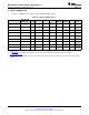
MSP430FR4133, MSP430FR4132, MSP430FR4131 SLAS865B – OCTOBER 2014 – REVISED AUGUST 2015 www.ti.com 3 Device Comparison Table 3-1 summarizes the features of the available family members. Table 3-1.
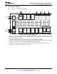
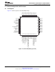
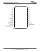
MSP430FR4133, MSP430FR4132, MSP430FR4131 www.ti.com SLAS865B – OCTOBER 2014 – REVISED AUGUST 2015 4 Terminal Configuration and Functions 4.1 Pin Diagrams 64 63 62 61 60 59 58 57 56 55 54 53 52 51 50 49 P7.0/L0 P7.1/L1 P7.2/L2 P7.3/L3 P7.4/L4 P7.5/L5 P7.6/L6 P7.7/L7 P3.0/L8 P3.1/L9 P3.2/L10 P3.3/L11 P3.4/L12 P3.5/L13 P3.6/L14 P3.7/L15 Figure 4-1 shows the pinout of the 64-pin PM package. 1 2 3 4 5 6 7 8 9 10 11 12 13 14 15 16 48 47 46 45 44 43 42 41 40 39 38 37 36 35 34 33 P6.0/L16 P6.1/L17 P6.
MSP430FR4133, MSP430FR4132, MSP430FR4131 SLAS865B – OCTOBER 2014 – REVISED AUGUST 2015 www.ti.com Figure 4-2 shows the pinout of the 56-pin DGG package. P7.5/L5 P7.4/L4 P7.3/L3 P7.2/L2 P7.1/L1 P7.0/L0 P4.7/R13 P4.6/R23 P4.5/R33 P4.4/LCDCAP1 P4.3/LCDCAP0 P4.2/XOUT P4.1/XIN DVSS DVCC RST/NMI/SBWTDIO TEST/SBWTCK P4.0/TA1.1 P8.3/TA1.2 P8.2/TA1CLK P1.7/TA0.1/TDO/A7 P1.6/TA0.2/TDI/TCLK/A6 P1.5/TA0CLK/TMS/A5 P1.4/MCLK/TCK/A4/VREF+ P1.3/UCA0STE/A3 P1.2/UCA0CLK/A2 P1.1/UCA0RXD/UCA0SOMI/A1/Veref+ P1.
MSP430FR4133, MSP430FR4132, MSP430FR4131 www.ti.com SLAS865B – OCTOBER 2014 – REVISED AUGUST 2015 Figure 4-3 shows the pinout of the 48-pin DGG package. P3.1/L9 P3.0/L8 P7.3/L3 P7.2/L2 P7.1/L1 P7.0/L0 P4.7/R13 P4.6/R23 P4.5/R33 P4.4/LCDCAP1 P4.3/LCDCAP0 P4.2/XOUT P4.1/XIN DVSS DVCC RST/NMI/SBWTDIO TEST/SBWTCK P4.0/TA1.1 P1.7/TA0.1/TDO/A7 P1.6/TA0.2/TDI/TCLK/A6 P1.5/TA0CLK/TMS/A5 P1.4/MCLK/TCK/A4/VREF+ P1.3/UCA0STE/A3 P1.
MSP430FR4133, MSP430FR4132, MSP430FR4131 SLAS865B – OCTOBER 2014 – REVISED AUGUST 2015 4.2 www.ti.com Signal Descriptions Table 4-1 describes the signals for all device variants and package options. Table 4-1. Signal Descriptions TERMINAL NAME PACKAGE SUFFIX I/O DESCRIPTION PM G56 G48 P4.7/R13 1 7 7 I/O General-purpose I/O Input/output port of third most positive analog LCD voltage V4 P4.
MSP430FR4133, MSP430FR4132, MSP430FR4131 www.ti.com SLAS865B – OCTOBER 2014 – REVISED AUGUST 2015 Table 4-1. Signal Descriptions (continued) TERMINAL NAME PACKAGE SUFFIX PM G56 I/O DESCRIPTION G48 P1.4/MCLK/TCK/A4/VREF+ 20 24 22 I/O General-purpose I/O (2) MCLK output Test clock Analog input A4 Output of positive reference voltage with ground as reference P1.3/UCA0STE/A3 21 25 23 I/O General-purpose I/O eUSCI_A0 SPI slave transmit enable Analog input A3 P1.
MSP430FR4133, MSP430FR4132, MSP430FR4131 SLAS865B – OCTOBER 2014 – REVISED AUGUST 2015 www.ti.com Table 4-1. Signal Descriptions (continued) TERMINAL NAME PACKAGE SUFFIX PM G56 I/O DESCRIPTION G48 (1) 41 I/O General-purpose I/O LCD drive pin; either segment or common output P6.6/L22 (1) 42 I/O General-purpose I/O LCD drive pin; either segment or common output P6.5/L21 (1) 43 43 I/O General-purpose I/O LCD drive pin; either segment or common output P6.
MSP430FR4133, MSP430FR4132, MSP430FR4131 www.ti.com 4.3 SLAS865B – OCTOBER 2014 – REVISED AUGUST 2015 Pin Multiplexing Pin multiplexing for these devices is controlled by both register settings and operating modes (for example, if the device is in test mode). For details of the settings for each pin and schematics of the multiplexed ports, see Section 6.9.13. 4.4 Connection of Unused Pins Table 4-2 shows the correct termination of unused pins. Table 4-2.
MSP430FR4133, MSP430FR4132, MSP430FR4131 SLAS865B – OCTOBER 2014 – REVISED AUGUST 2015 www.ti.com 5 Specifications Absolute Maximum Ratings (1) 5.1 over operating free-air temperature range (unless otherwise noted) MIN MAX Voltage applied at DVCC pin to VSS –0.3 4.1 UNIT V Voltage applied to any pin (2) –0.3 VCC + 0.3 (4.
MSP430FR4133, MSP430FR4132, MSP430FR4131 www.ti.com 5.
MSP430FR4133, MSP430FR4132, MSP430FR4131 SLAS865B – OCTOBER 2014 – REVISED AUGUST 2015 5.7 www.ti.com Low-Power Mode LPM3, LPM4 Supply Currents (Into VCC) Excluding External Current over recommended ranges of supply voltage and operating free-air temperature (unless otherwise noted) PARAMETER TYP 1.99 3.00 MAX UNIT 1.21 3V 0.92 1.00 2V 0.86 1.00 2.75 Low-power mode 3, LCD, excludes SVS (6) 3V 1.07 1.25 3.04 µA RTC Low-power mode 3, RTC, excludes SVS (7) 3V 1.08 1.25 3.
MSP430FR4133, MSP430FR4132, MSP430FR4131 www.ti.com 5.8 SLAS865B – OCTOBER 2014 – REVISED AUGUST 2015 Low-Power Mode LPMx.5 Supply Currents (Into VCC) Excluding External Current over recommended ranges of supply voltage and operating free-air temperature (unless otherwise noted) PARAMETER ILPM3.5, XT1 Low-power mode 3.5, includes SVS (1) (2) (also refer to Figure 5-3) ILPM3.5, LCD, CP Low-power mode 3.5, excludes SVS (4) ILPM4.5, Low-power mode 4.5, includes SVS (5) ILPM4.
MSP430FR4133, MSP430FR4132, MSP430FR4131 SLAS865B – OCTOBER 2014 – REVISED AUGUST 2015 5.9 www.ti.com Typical Characteristics, Low-Power Mode Supply Currents 5 5 4.5 4.5 LPM3 Supply Current (µA) LPM3 Supply Current (µA) The graphs in this section show only board-level test result on a small number of samples. A MS1V-T1K crystal from Micro-Crystal was populated for 32-kHz clock generation. LCD is configured in 4xCOM mode without LCD panel populated. 4 3.5 3 2.5 2 1.5 1 4 3.5 3 2.5 2 1.5 1 0.5 0.
MSP430FR4133, MSP430FR4132, MSP430FR4131 www.ti.com SLAS865B – OCTOBER 2014 – REVISED AUGUST 2015 5.10 Typical Characteristics, Current Consumption Per Module MODULE TEST CONDITIONS REFERENCE CLOCK Timer_A TYP UNIT Module input clock 5 µA/MHz eUSCI_A UART mode Module input clock 7 µA/MHz eUSCI_A SPI mode Module input clock 5 µA/MHz eUSCI_B SPI mode Module input clock 5 µA/MHz Module input clock 5 µA/MHz 32 kHz 85 nA MCLK 8.
MSP430FR4133, MSP430FR4132, MSP430FR4131 SLAS865B – OCTOBER 2014 – REVISED AUGUST 2015 www.ti.com 5.12 Timing and Switching Characteristics 5.12.1 Power Supply Sequencing V Power Cycle Reset SVS Reset V SVS+ BOR Reset V SVS– V BOR t BOR t Figure 5-5. Power Cycle, SVS, and BOR Reset Conditions Table 5-1.
MSP430FR4133, MSP430FR4132, MSP430FR4131 www.ti.com SLAS865B – OCTOBER 2014 – REVISED AUGUST 2015 5.12.2 Reset Timing Table 5-2.
MSP430FR4133, MSP430FR4132, MSP430FR4131 SLAS865B – OCTOBER 2014 – REVISED AUGUST 2015 www.ti.com 5.12.3 Clock Specifications Table 5-3.
MSP430FR4133, MSP430FR4132, MSP430FR4131 www.ti.com SLAS865B – OCTOBER 2014 – REVISED AUGUST 2015 Table 5-4. DCO FLL, Frequency Over recommended operating free-air temperature (unless otherwise noted) PARAMETER TEST CONDITIONS FLL lock frequency, 16 MHz, 25°C fDCO, FLL lock frequency, 16 MHz, –40°C to +85°C Measured at MCLK, Internal trimmed REFO as reference VCC MIN 3V –1.0% TYP 1.0% MAX 3V –2.0% 2.0% 3V –0.5% 0.
MSP430FR4133, MSP430FR4132, MSP430FR4131 SLAS865B – OCTOBER 2014 – REVISED AUGUST 2015 www.ti.com 5.12.4 Digital I/Os Table 5-8. Digital Inputs over recommended ranges of supply voltage and operating free-air temperature (unless otherwise noted) PARAMETER TEST CONDITIONS VCC MIN 2V 0.90 TYP MAX 1.50 3V 1.35 2.25 2V 0.50 1.10 3V 0.75 1.65 2V 0.3 0.8 3V 0.4 1.
MSP430FR4133, MSP430FR4132, MSP430FR4131 www.ti.com SLAS865B – OCTOBER 2014 – REVISED AUGUST 2015 5.12.4.1 Digital I/O Typical Characteristics 10 Low-Level Output Current (mA) Low-Level Output Current (mA) 25 T A = 85°C 20 T A = 25°C 15 10 5 0 T A = 85°C T A = 25°C 7.5 5 2.5 0 0 0.5 1 1.5 2 Low-Level Output Voltage (V) 2.5 3 0 DVCC = 3 V 0.5 0.75 1 1.25 1.5 Low-Level Output Voltage (V) 1.75 2 DVCC = 2 V Figure 5-6.
MSP430FR4133, MSP430FR4132, MSP430FR4131 SLAS865B – OCTOBER 2014 – REVISED AUGUST 2015 www.ti.com 5.12.6 eUSCI Table 5-11.
MSP430FR4133, MSP430FR4132, MSP430FR4131 www.ti.com SLAS865B – OCTOBER 2014 – REVISED AUGUST 2015 1/fUCxCLK CKPL = 0 UCLK CKPL = 1 tLOW/HIGH tLOW/HIGH tSU,MI tHD,MI SOMI tVALID,MO SIMO Figure 5-10. SPI Master Mode, CKPH = 0 1/fUCxCLK CKPL = 0 UCLK CKPL = 1 tLOW/HIGH tLOW/HIGH tSU,MI tHD,MI SOMI tVALID,MO SIMO Figure 5-11.
MSP430FR4133, MSP430FR4132, MSP430FR4131 SLAS865B – OCTOBER 2014 – REVISED AUGUST 2015 www.ti.com Table 5-15.
MSP430FR4133, MSP430FR4132, MSP430FR4131 www.ti.com SLAS865B – OCTOBER 2014 – REVISED AUGUST 2015 tSTE,LAG tSTE,LEAD STE 1/fUCxCLK CKPL = 0 UCLK CKPL = 1 tLOW/HIGH tSU,SIMO tLOW/HIGH tHD,SIMO SIMO tACC tDIS tVALID,SOMI SOMI Figure 5-12. SPI Slave Mode, CKPH = 0 tSTE,LAG tSTE,LEAD STE 1/fUCxCLK CKPL = 0 UCLK CKPL = 1 tLOW/HIGH tLOW/HIGH tHD,SI tSU,SI SIMO tACC tVALID,SO tDIS SOMI Figure 5-13.
MSP430FR4133, MSP430FR4132, MSP430FR4131 SLAS865B – OCTOBER 2014 – REVISED AUGUST 2015 www.ti.com Table 5-16. eUSCI (I2C Mode) Switching Characteristics over recommended ranges of supply voltage and operating free-air temperature (unless otherwise noted) (see Figure 5-14) PARAMETER TEST CONDITIONS feUSCI eUSCI input clock frequency fSCL SCL clock frequency VCC MIN TYP Internal: SMCLK, MODCLK External: UCLK Duty cycle = 50% ±10% 2 V, 3 V fSCL = 100 kHz UNIT 16 MHz 400 kHz 4.
MSP430FR4133, MSP430FR4132, MSP430FR4131 www.ti.com SLAS865B – OCTOBER 2014 – REVISED AUGUST 2015 5.12.7 ADC Table 5-17.
MSP430FR4133, MSP430FR4132, MSP430FR4131 SLAS865B – OCTOBER 2014 – REVISED AUGUST 2015 www.ti.com Table 5-19.
MSP430FR4133, MSP430FR4132, MSP430FR4131 www.ti.com SLAS865B – OCTOBER 2014 – REVISED AUGUST 2015 5.12.8 LCD Controller Table 5-20. LCD Recommended Operating Conditions over operating free-air temperature range (unless otherwise noted) PARAMETER CONDITIONS VCC,LCD,CP en,3.6 LCDCPEN = 1, 0000 < VLCDx ≤ 1111, Supply voltage range, charge pump LCDREFEN = 1 (charge pump enabled, enabled, VLCD ≤ 3.6 V VLCD ≤ 3.6 V) VCC,LCD,ext.
MSP430FR4133, MSP430FR4132, MSP430FR4131 SLAS865B – OCTOBER 2014 – REVISED AUGUST 2015 www.ti.com 5.12.9 FRAM Table 5-21. FRAM over recommended ranges of supply voltage and operating free-air temperature (unless otherwise noted) PARAMETER TEST CONDITIONS MIN tRetention MAX 1015 Read and write endurance Data retention duration TJ = 25°C 100 TJ = 70°C 40 TJ = 85°C 10 UNIT cycles years 5.12.10 Emulation and Debug Table 5-22.
MSP430FR4133, MSP430FR4132, MSP430FR4131 www.ti.com SLAS865B – OCTOBER 2014 – REVISED AUGUST 2015 6 Detailed Description 6.1 CPU The MSP430 CPU has a 16-bit RISC architecture that is highly transparent to the application. All operations, other than program-flow instructions, are performed as register operations in conjunction with seven addressing modes for source operand and four addressing modes for destination operand.
MSP430FR4133, MSP430FR4132, MSP430FR4131 SLAS865B – OCTOBER 2014 – REVISED AUGUST 2015 www.ti.com Table 6-1. Operating Modes (continued) AM LPM4 LPM3.5 LPM4.
MSP430FR4133, MSP430FR4132, MSP430FR4131 www.ti.com SLAS865B – OCTOBER 2014 – REVISED AUGUST 2015 Table 6-2.
MSP430FR4133, MSP430FR4132, MSP430FR4131 SLAS865B – OCTOBER 2014 – REVISED AUGUST 2015 www.ti.com Table 6-4. JTAG Pin Requirements and Function 6.6 DEVICE SIGNAL DIRECTION P1.4/MCLK/TCK/A4/VREF+ IN JTAG FUNCTION JTAG clock input P1.5/TA0CLK/TMS/A5 IN JTAG state control P1.6/TA0.2/TDI/TCLK/A6 IN JTAG data input/TCLK input P1.7/TA0.
MSP430FR4133, MSP430FR4132, MSP430FR4131 www.ti.com 6.9 SLAS865B – OCTOBER 2014 – REVISED AUGUST 2015 Peripherals Peripherals are connected to the CPU through data, address, and control buses. All peripherals can be handled by using all instructions in the memory map. For complete module description, see the MSP430FR4xx and MSP430FR2xx Family User's Guide (SLAU445). 6.9.
MSP430FR4133, MSP430FR4132, MSP430FR4131 SLAS865B – OCTOBER 2014 – REVISED AUGUST 2015 www.ti.com Table 6-6.
MSP430FR4133, MSP430FR4132, MSP430FR4131 www.ti.com 6.9.4 SLAS865B – OCTOBER 2014 – REVISED AUGUST 2015 Watchdog Timer (WDT) The primary function of the WDT module is to perform a controlled system restart after a software problem occurs. If the selected time interval expires, a system reset is generated. If the watchdog function is not needed in an application, the module can be configured as interval timer and can generate interrupts at selected time intervals. Table 6-7. WDT Clocks 6.9.
MSP430FR4133, MSP430FR4132, MSP430FR4131 SLAS865B – OCTOBER 2014 – REVISED AUGUST 2015 www.ti.com Table 6-8. System Module Interrupt Vector Registers (continued) INTERRUPT VECTOR REGISTER SYSSNIV, System NMI SYSUNIV, User NMI 6.9.
MSP430FR4133, MSP430FR4132, MSP430FR4131 www.ti.com 6.9.8 SLAS865B – OCTOBER 2014 – REVISED AUGUST 2015 Timers (Timer0_A3, Timer1_A3) The Timer0_A3 and Timer1_A3 modules are 16-bit timers and counters with three capture/compare registers each. Each can support multiple captures or compares, PWM outputs, and interval timing. Each has extensive interrupt capabilities. Interrupts may be generated from the counter on overflow conditions and from each of the capture/compare registers.
MSP430FR4133, MSP430FR4132, MSP430FR4131 SLAS865B – OCTOBER 2014 – REVISED AUGUST 2015 www.ti.com Table 6-11. Timer1_A3 Signal Connections PORT PIN DEVICE INPUT SIGNAL MODULE INPUT NAME P8.2 TA1CLK TACLK ACLK (internal) ACLK SMCLK (internal) SMCLK Timer0_A3 CCR2B output (internal) INCLK MODULE BLOCK MODULE OUTPUT SIGNAL Timer N/A CCR0 TA0 DEVICE OUTPUT SIGNAL CCI0A Timer0_A3 CCR0B output (internal) CCI0B DVSS GND DVCC VCC TA1.
MSP430FR4133, MSP430FR4132, MSP430FR4131 www.ti.com 6.9.9 SLAS865B – OCTOBER 2014 – REVISED AUGUST 2015 Real-Time Clock (RTC) Counter The RTC counter is a 16-bit modulo counter that is functional in AM, LPM0, LPM3, and LPM3.5. This module may periodically wake up the CPU from LPM0, LPM3, and LPM3.5 based on timing from a lowpower clock source such as the XT1 and VLO clocks. In AM, RTC can be driven by SMCLK to generate high-frequency timing events and interrupts.
MSP430FR4133, MSP430FR4132, MSP430FR4131 SLAS865B – OCTOBER 2014 – REVISED AUGUST 2015 www.ti.com 6.9.11 Liquid Crystal Display (LCD) The LCD driver generates the segment and common signals to drive segment liquid crystal display (LCD) glass. The LCD controller has dedicated data memories to hold segment drive information. Common and segment signals are generated as defined by the mode. Static, 2-mux, 3-mux, up to 8-mux LCDs are supported.
MSP430FR4133, MSP430FR4132, MSP430FR4131 www.ti.com SLAS865B – OCTOBER 2014 – REVISED AUGUST 2015 6.9.13 Input/Output Schematics 6.9.13.1 Port P1 Input/Output With Schmitt Trigger A0..A7 From ADC A P1REN.x P1DIR.x 0 From Module 1 DVSS 0 DVCC 1 P1OUT.x 0 From Module 1 P1SEL0.x EN To module D P1IN.x P1IE.x P1 Interrupt Q D S P1IFG.x Edge Select P1IES.x From JTAG Bus Keeper P1.0/UCA0TXD/UCA0SIMO/A0 P1.1/UCA0RXD/UCA0SOMI/A1 P1.2/UCA0CLK/A2 P1.3/UCA0STE/A3 P1.4/MCLK/TCK/A4/VREF+ P1.
MSP430FR4133, MSP430FR4132, MSP430FR4131 SLAS865B – OCTOBER 2014 – REVISED AUGUST 2015 www.ti.com Table 6-14. Port P1 Pin Functions PIN NAME (P1.x) x FUNCTION P1.0 (I/O) P1.0/UCA0TXD/ UCA0SIMO/A0 0 UCA0TXD/UCA0SIMO A0 P1.1 (I/O) P1.1/UCA0RXD/ UCA0SOMI/A1 1 UCA0RXD/UCA0SOMI A1 P1.2/UCA0CLK/A2 2 3 P1.
MSP430FR4133, MSP430FR4132, MSP430FR4131 www.ti.com SLAS865B – OCTOBER 2014 – REVISED AUGUST 2015 6.9.13.2 Port P2 Input/Output With Schmitt Trigger L24..L31 From LCD P2REN.x P2DIR.x DVSS 0 DVCC 1 P2OUT.x P2IN.x P2IE.x P2 Interrupt Q D S P2IFG.x 1 P2IES.x Edge Select 1 Bus Keeper P2.0/L24 P2.1/L25 P2.2/L26 P2.3/L27 P2.4/L28 P2.5/L29 P2.6/L30 P2.7/L31 Figure 6-3.
MSP430FR4133, MSP430FR4132, MSP430FR4131 SLAS865B – OCTOBER 2014 – REVISED AUGUST 2015 www.ti.com Table 6-15. Port P2 Pin Functions PIN NAME (P2.x) P2.0/L24 P2.1/L25 P2.2/L26 x 0 1 2 3 P2.4/L28 4 P2.5/L29 5 P2.6/L30 6 P2.7/L31 7 50 P2.0 (I/O) L24 P2.1 (I/O) L25 P2.3/L27 (1) FUNCTION P2.2 (I/O) L26 P2.3 (I/O) L27 P2.4 (I/O) L28 P2.5 (I/O) L29 P2.6 (I/O) L30 P2.7 (I/O) L31 CONTROL BITS AND SIGNALS (1) P2DIR.
MSP430FR4133, MSP430FR4132, MSP430FR4131 www.ti.com SLAS865B – OCTOBER 2014 – REVISED AUGUST 2015 6.9.13.3 Port P3 Input/Output With Schmitt Trigger L8..L15 From LCD E P3REN.x P3DIR.x DVSS 0 DVCC 1 P3OUT.x P3IN.x Bus Keeper P3.0/L8 P3.1/L9 P3.2/L10 P3.3/L11 P3.4/L12 P3.5/L13 P3.6/L14 P3.7/L15 Figure 6-4.
MSP430FR4133, MSP430FR4132, MSP430FR4131 SLAS865B – OCTOBER 2014 – REVISED AUGUST 2015 www.ti.com Table 6-16. Port P3 Pin Functions PIN NAME (P3.x) x P3.0/L8 0 P3.1/L9 1 P3.2/L10 2 P3.3/L11 3 P3.4/L12 4 P3.5/L13 5 P3.6/L14 6 P3.7/L15 7 (1) 52 FUNCTION P3.0 (I/O) L8 P3.1 (I/O) L9 P3.2 (I/O) L10 P3.3 (I/O) L11 P3.4 (I/O) L12 P3.5 (I/O) L13 P3.6 (I/O) L14 P3.7 (I/O) L15 CONTROL BITS AND SIGNALS (1) P3DIR.
MSP430FR4133, MSP430FR4132, MSP430FR4131 www.ti.com SLAS865B – OCTOBER 2014 – REVISED AUGUST 2015 6.9.13.4 Port P4.0 Input/Output With Schmitt Trigger P4REN.x P4DIR.x 0 From Module 1 DVSS 0 DVCC 1 P4OUT.x 0 From Module 1 P4SEL0.x EN D To module P4IN.x Bus Keeper P4.0/TA1.1 Figure 6-5. Port P4.0 Input/Output With Schmitt Trigger Table 6-17. Port P4.0 Pin Functions PIN NAME (P4.x) x FUNCTION P4.0 (I/O) P4.0/TA1.1 0 CONTROL BITS AND SIGNALS P4DIR.x P4SEL0.x I: 0; O: 1 0 TA1.
MSP430FR4133, MSP430FR4132, MSP430FR4131 SLAS865B – OCTOBER 2014 – REVISED AUGUST 2015 www.ti.com 6.9.13.5 Port P4.1 and P4.2 Input/Output With Schmitt Trigger XIN, XOUT P4REN.x P4DIR.x DVSS 0 DVCC 1 P4OUT.x P4SEL0.x P4IN.x Bus Keeper P4.1/XIN P4.2/XOUT Figure 6-6. Port P4.1 and P4.2 Input/Output With Schmitt Trigger Table 6-18. Port P4.1 and P4.2 Pin Functions PIN NAME (P4.x) P4.1/XIN P4.2/XOUT (1) 54 x 1 2 FUNCTION P4.1 (I/O) XIN P4.2 (I/O) XOUT CONTROL BITS AND SIGNALS (1) P4DIR.
MSP430FR4133, MSP430FR4132, MSP430FR4131 www.ti.com SLAS865B – OCTOBER 2014 – REVISED AUGUST 2015 6.9.13.6 Port 4.3, P4.4, P4.5, P4.6, and P4.7 Input/Output With Schmitt Trigger LCDCAP0, LCDCAP1 R13, R23, R33 From LCD P4REN.x P4DIR.x DVSS 0 DVCC 1 P4OUT.x P4IN.x Bus Keeper P4.3/LCDCAP0 P4.4/LCDCAP1 P4.5/R33 P4.6/R23 P4.7/R13 Figure 6-7. Port 4.3, P4.4, P4.5, P4.6, and P4.
MSP430FR4133, MSP430FR4132, MSP430FR4131 SLAS865B – OCTOBER 2014 – REVISED AUGUST 2015 www.ti.com Table 6-19. Port P4.3, P4.4, P4.5, P4.6, and P4.7 Pin Functions PIN NAME (P4.x) x P4.3/LCDCAP0 3 P4.4/LCDCAP1 4 P4.5/R33 5 P4.6/R23 6 P4.7/R13 7 (1) (2) 56 FUNCTION CONTROL BITS AND SIGNALS (1) P4DIR.x LCDPCTL (2) P4.3 (I/O) I: 0; O: 1 X LCDCAP0 X 1 P4.4 (I/O) I: 0; O: 1 0 LCDCAP1 X 1 P4.5 (I/O) I: 0; O: 1 0 R33 P4.6 (I/O) R23 P4.
MSP430FR4133, MSP430FR4132, MSP430FR4131 www.ti.com SLAS865B – OCTOBER 2014 – REVISED AUGUST 2015 6.9.13.7 Port P5.0, P5.1, P5.2, and P5.3 Input/Output With Schmitt Trigger L32..L35 From LCD E P5REN.x P5DIR.x 0 From Module 1 DVSS 0 DVCC 1 P5OUT.x 0 From Module 1 P5SEL0.x EN To module D P5IN.x Bus Keeper P5.0/UCB0STE/L32 P5.1/UCB0CLK/L33 P5.2/UCB0SIMO/UCB0SDA/L34 P5.3/UCB0SOMI/UCB0SCL/L35 Figure 6-8. Port P5.0, P5.1, P5.2, and P5.
MSP430FR4133, MSP430FR4132, MSP430FR4131 SLAS865B – OCTOBER 2014 – REVISED AUGUST 2015 www.ti.com Table 6-20. Port P5.0, P5.1, P5.2, and P5.3 Pin Functions PIN NAME (P5.x) P5.0/UCB0STE/L32 x 0 FUNCTION P5DIR.x P5SEL0.x LCDSy P5.0 (I/O) I: 0; O: 1 0 0 UCB0STE 0 1 0 L32 P5.1/UCB0CLK/L33 1 X X 1 (y = 32) P5.1 (I/O) I: 0; O: 1 0 0 UCB0CLK 0 1 0 L33 P5.2 (I/O) P5.
MSP430FR4133, MSP430FR4132, MSP430FR4131 www.ti.com SLAS865B – OCTOBER 2014 – REVISED AUGUST 2015 6.9.13.8 Port P5.4, P5.5, P5.6, and P5.7 Input/Output With Schmitt Trigger L36..L39 From LCD E P5REN.x P5DIR.x DVSS 0 DVCC 1 P5OUT.x P5IN.x Bus Keeper P5.4/L36 P5.5/L37 P5.6/L38 P5.7/L39 Figure 6-9. Port P5.4, P5.5, P5.6, and P5.
MSP430FR4133, MSP430FR4132, MSP430FR4131 SLAS865B – OCTOBER 2014 – REVISED AUGUST 2015 www.ti.com Table 6-21. Port P5.4, P5.5, P5.6, and P5.7 Pin Functions PIN NAME (P5.x) x P5.4/L36 4 P5.5/L37 5 P5.6/L38 6 P5.7/L39 (1) 60 7 FUNCTION P5.4 (I/O) L36 P5.5 (I/O) L37 P5.6 (I/O) L38 P5.7 (I/O) L39 CONTROL BITS AND SIGNALS (1) P5DIR.
MSP430FR4133, MSP430FR4132, MSP430FR4131 www.ti.com SLAS865B – OCTOBER 2014 – REVISED AUGUST 2015 6.9.13.9 Port P6 Input/Output With Schmitt Trigger L16..L23 From LCD E P6REN.x P6DIR.x DVSS 0 DVCC 1 P6OUT.x P6IN.x Bus Keeper P6.0/L16 P6.1/L17 P6.2/L18 P6.3/L19 P6.4/L20 P6.5/L21 P6.6/L22 P6.7/L23 Figure 6-10.
MSP430FR4133, MSP430FR4132, MSP430FR4131 SLAS865B – OCTOBER 2014 – REVISED AUGUST 2015 www.ti.com Table 6-22. Port P6 Pin Functions PIN NAME (P6.x) x P6.0/L16 0 P6.1/L17 1 P6.2/L18 2 P6.3/L19 3 P6.4/L20 4 P6.5/L21 5 P6.6/L22 6 P6.7/L23 7 (1) 62 FUNCTION P6.0 (I/O) L16 P6.1 (I/O) L17 P6.2 (I/O) L18 P6.3 (I/O) L19 P6.4 (I/O) L20 P6.5 (I/O) L21 P6.6 (I/O) L22 P6.7 (I/O) L23 CONTROL BITS AND SIGNALS (1) P6DIR.
MSP430FR4133, MSP430FR4132, MSP430FR4131 www.ti.com SLAS865B – OCTOBER 2014 – REVISED AUGUST 2015 6.9.13.10 Port P7 Input/Output With Schmitt Trigger L0..L7 From LCD E P7REN.x P7DIR.x DVSS 0 DVCC 1 P7OUT.x P7IN.x Bus Keeper P7.0/L0 P7.1/L1 P7.2/L2 P7.3/L3 P7.4/L4 P7.5/L5 P7.6/L6 P7.7/L7 Figure 6-11.
MSP430FR4133, MSP430FR4132, MSP430FR4131 SLAS865B – OCTOBER 2014 – REVISED AUGUST 2015 www.ti.com Table 6-23. Port P7 Pin Functions PIN NAME (P7.x) x P7.0/L0 0 P7.1/L1 1 P7.2/L2 2 P7.3/L3 3 P7.4/L4 4 P7.5/L5 5 P7.6/L6 6 P7.7/L7 7 (1) 64 FUNCTION P7.0 (I/O) L0 P7.1 (I/O) L1 P7.2 (I/O) L2 P7.3 (I/O) L3 P7.4 (I/O) L4 P7.5 (I/O) L5 P7.6 (I/O) L6 P7.7 (I/O) L7 CONTROL BITS AND SIGNALS (1) P7DIR.
MSP430FR4133, MSP430FR4132, MSP430FR4131 www.ti.com SLAS865B – OCTOBER 2014 – REVISED AUGUST 2015 6.9.13.11 Port P8.0 and P8.1 Input/Output With Schmitt Trigger A8..9 From ADC A P8REN.x P8DIR.x 0 From Module 1 DVSS 0 DVCC 1 P8OUT.x 0 From MCLK, ACLK 1 P8SEL0.x EN To module D P8IN.x Bus Keeper P8.0/SMCLK/A8 P8.1/ACLK/A9 Figure 6-12. Port P8.0 and P8.
MSP430FR4133, MSP430FR4132, MSP430FR4131 SLAS865B – OCTOBER 2014 – REVISED AUGUST 2015 www.ti.com Table 6-24. Port P8.0 and P8.1 Pin Functions PIN NAME (P8.x) x FUNCTION P8.0 (I/O) P8.0/SMCLK/A8 0 (1) (2) 66 P8SEL0.x ADCPCTLx (2) I: 0; O: 1 0 0 1 0 X X 1 (x = 8) I: 0; O: 1 0 0 1 0 X 1 (x = 9) 0 SMCLK 1 P8.1 (I/O) 1 P8DIR.x VSS A8 P8.
MSP430FR4133, MSP430FR4132, MSP430FR4131 www.ti.com SLAS865B – OCTOBER 2014 – REVISED AUGUST 2015 6.9.13.12 Port P8.2 and P8.3 Input/Output With Schmitt Trigger P8REN.x P8DIR.x 0 From Module 1 DVSS 0 DVCC 1 P8OUT.x 0 From Module 1 P8SEL0.x EN D To module P8IN.x Bus Keeper P8.2/TA1CLK P8.3/TA1.2 Figure 6-13. Port P8.2 and P8.3 Input/Output With Schmitt Trigger Table 6-25. Port P8.2 and P8.3 Pin Functions PIN NAME (P8.x) P8.2/TA1CLK x 2 FUNCTION P8SEL0.x P8.
MSP430FR4133, MSP430FR4132, MSP430FR4131 SLAS865B – OCTOBER 2014 – REVISED AUGUST 2015 www.ti.com 6.10 Device Descriptors (TLV) Table 6-26 lists the Device IDs of the MSP430FR413x devices. Table 6-27 lists the contents of the device descriptor tag-length-value (TLV) structure for the MSP430FR413x devices. Table 6-26. Device IDs DEVICE ID DEVICE 1A04h 1A05h MSP430FR4133 F0h 81h MSP430FR4132 F1h 81h MSP430FR4131 F2h 81h Table 6-27.
MSP430FR4133, MSP430FR4132, MSP430FR4131 www.ti.com SLAS865B – OCTOBER 2014 – REVISED AUGUST 2015 Table 6-27. Device Descriptors (continued) MSP430FR413x DESCRIPTION ADDRESS VALUE Calibration Tag 1A1Eh 12h Calibration Length 1A1Fh 04h 1A20h per unit 1A21h per unit 1A22h per unit 1A23h per unit Reference and DCO Calibration 1.
MSP430FR4133, MSP430FR4132, MSP430FR4131 SLAS865B – OCTOBER 2014 – REVISED AUGUST 2015 www.ti.com 6.11.1 Peripheral File Map Table 6-29 shows the base address and the memory size of the registers of each peripheral, and Table 630 through Table 6-49 show all of the available registers for each peripheral and their address offsets. Table 6-29.
MSP430FR4133, MSP430FR4132, MSP430FR4131 www.ti.com SLAS865B – OCTOBER 2014 – REVISED AUGUST 2015 Table 6-30. Special Function Registers (Base Address: 0100h) REGISTER DESCRIPTION SFR interrupt enable SFR interrupt flag SFR reset pin control REGISTER OFFSET SFRIE1 00h SFRIFG1 02h SFRRPCR 04h Table 6-31.
MSP430FR4133, MSP430FR4132, MSP430FR4131 SLAS865B – OCTOBER 2014 – REVISED AUGUST 2015 www.ti.com Table 6-35. CRC Registers (Base Address: 01C0h) REGISTER OFFSET CRC data input REGISTER DESCRIPTION CRC16DI 00h CRC data input reverse byte CRCDIRB 02h CRC initialization and result CRCINIRES 04h CRC result reverse byte CRCRESR 06h Table 6-36. WDT Registers (Base Address: 01CCh) REGISTER DESCRIPTION Watchdog timer control REGISTER OFFSET WDTCTL 00h Table 6-37.
MSP430FR4133, MSP430FR4132, MSP430FR4131 www.ti.com SLAS865B – OCTOBER 2014 – REVISED AUGUST 2015 Table 6-39.
MSP430FR4133, MSP430FR4132, MSP430FR4131 SLAS865B – OCTOBER 2014 – REVISED AUGUST 2015 www.ti.com Table 6-43.
MSP430FR4133, MSP430FR4132, MSP430FR4131 www.ti.com SLAS865B – OCTOBER 2014 – REVISED AUGUST 2015 Table 6-46.
MSP430FR4133, MSP430FR4132, MSP430FR4131 SLAS865B – OCTOBER 2014 – REVISED AUGUST 2015 www.ti.com Table 6-47.
MSP430FR4133, MSP430FR4132, MSP430FR4131 www.ti.com SLAS865B – OCTOBER 2014 – REVISED AUGUST 2015 Table 6-49.
MSP430FR4133, MSP430FR4132, MSP430FR4131 SLAS865B – OCTOBER 2014 – REVISED AUGUST 2015 www.ti.com 7 Applications, Implementation, and Layout NOTE Information in the following applications sections is not part of the TI component specification, and TI does not warrant its accuracy or completeness. TI’s customers are responsible for determining suitability of components for their purposes. Customers should validate and test their design implementation to confirm system functionality. 7.
MSP430FR4133, MSP430FR4132, MSP430FR4131 www.ti.com 7.1.3 SLAS865B – OCTOBER 2014 – REVISED AUGUST 2015 JTAG With the proper connections, the debugger and a hardware JTAG interface (such as the MSP-FET or MSP-FET430UIF) can be used to program and debug code on the target board. In addition, the connections also support the MSP-GANG production programmers, thus providing an easy way to program prototype boards, if desired.
MSP430FR4133, MSP430FR4132, MSP430FR4131 SLAS865B – OCTOBER 2014 – REVISED AUGUST 2015 www.ti.com VCC Important to connect MSP430FRxxx J1 (see Note A) DVCC J2 (see Note A) R1 47 kΩ (see Note B) JTAG VCC TOOL VCC TARGET 2 1 4 3 6 5 8 7 10 9 12 11 14 13 TDO/TDI RST/NMI/SBWTDIO TCK GND TEST/SBWTCK C1 1 nF (see Note B) A. B. DVSS Make connection J1 if a local target power supply is used, or make connection J2 if the target is powered from the debug or programming adapter.
MSP430FR4133, MSP430FR4132, MSP430FR4131 www.ti.com 7.1.6 SLAS865B – OCTOBER 2014 – REVISED AUGUST 2015 General Layout Recommendations • • • • • 7.1.7 Proper grounding and short traces for external crystal to reduce parasitic capacitance. See the application report MSP430 32-kHz Crystal Oscillators (SLAA322) for recommended layout guidelines. Proper bypass capacitors on DVCC and reference pins, if used. Avoid routing any high-frequency signal close to an analog signal line.
MSP430FR4133, MSP430FR4132, MSP430FR4131 SLAS865B – OCTOBER 2014 – REVISED AUGUST 2015 www.ti.com Figure 7-5 shows the recommended decoupling circuit when an external voltage reference is used. The internal reference module has a maximum drive current as described in the sections ADC Pin Enable and 1.2-V Reference Settings of the MSP430FR4xx and MSP430FR2xx Family User's Guide (SLAU445). The reference voltage must be a stable voltage for accurate measurements.
MSP430FR4133, MSP430FR4132, MSP430FR4131 www.ti.com SLAS865B – OCTOBER 2014 – REVISED AUGUST 2015 Table 7-1.
MSP430FR4133, MSP430FR4132, MSP430FR4131 SLAS865B – OCTOBER 2014 – REVISED AUGUST 2015 www.ti.com consecutive LCDMx registers. This allows use of simple look-up tables or software loops to output numbers on an LCD, reducing computational overhead and optimizing the energy consumption of an application.
MSP430FR4133, MSP430FR4132, MSP430FR4131 www.ti.com SLAS865B – OCTOBER 2014 – REVISED AUGUST 2015 8 Device and Documentation Support 8.1 Device Support 8.1.1 Development Tools Support 8.1.1.1 Hardware Features See the Code Composer Studio for MSP430 User's Guide (SLAU157) for details on the available features. MSP430 ARCHITECTURE 4-WIRE JTAG 2-WIRE JTAG BREAKPOINTS (N) RANGE BREAKPOINTS CLOCK CONTROL STATE SEQUENCER TRACE BUFFER LPMX.
MSP430FR4133, MSP430FR4132, MSP430FR4131 SLAS865B – OCTOBER 2014 – REVISED AUGUST 2015 www.ti.com 8.1.1.3.2 MSP430Ware MSP430Ware is a collection of code examples, data sheets, and other design resources for all MSP430 devices delivered in a convenient package. In addition to providing a complete collection of existing MSP430 design resources, MSP430Ware also includes a high-level API called MSP430 Driver Library. This library makes it easy to program MSP430 hardware.
MSP430FR4133, MSP430FR4132, MSP430FR4131 www.ti.com SLAS865B – OCTOBER 2014 – REVISED AUGUST 2015 8.1.2.2.2.4 Production Programmers The production programmers expedite loading firmware to devices by programming several devices simultaneously. PART NUMBER PC PORT FEATURES PROVIDER MSP-GANG Serial and USB Program up to eight devices at a time. Works with PC or as a stand-alone device. Texas Instruments 8.1.2.2.3 Recommended Software Options 8.1.2.2.3.
MSP430FR4133, MSP430FR4132, MSP430FR4131 SLAS865B – OCTOBER 2014 – REVISED AUGUST 2015 www.ti.com Predictions show that prototype devices (XMS) have a greater failure rate than the standard production devices. TI recommends that these devices not be used in any production system because their expected end-use failure rate still is undefined. Only qualified production devices are to be used. TI device nomenclature also includes a suffix with the device family name.
MSP430FR4133, MSP430FR4132, MSP430FR4131 www.ti.com 8.2.1 SLAS865B – OCTOBER 2014 – REVISED AUGUST 2015 Related Links Table 8-1 lists quick access links. Categories include technical documents, support and community resources, tools and software, and quick access to sample or buy. Table 8-1.
MSP430FR4133, MSP430FR4132, MSP430FR4131 SLAS865B – OCTOBER 2014 – REVISED AUGUST 2015 www.ti.com 9 Mechanical, Packaging, and Orderable Information 9.1 Packaging Information The following pages include mechanical, packaging, and orderable information. This information is the most current data available for the designated devices. This data is subject to change without notice and revision of this document. For browser-based versions of this data sheet, refer to the left-hand navigation.
PACKAGE OPTION ADDENDUM www.ti.
PACKAGE OPTION ADDENDUM www.ti.com 23-Apr-2015 LIFEBUY: TI has announced that the device will be discontinued, and a lifetime-buy period is in effect. NRND: Not recommended for new designs. Device is in production to support existing customers, but TI does not recommend using this part in a new design. PREVIEW: Device has been announced but is not in production. Samples may or may not be available. OBSOLETE: TI has discontinued the production of the device.
PACKAGE MATERIALS INFORMATION www.ti.com 5-Aug-2015 TAPE AND REEL INFORMATION *All dimensions are nominal Device Package Package Pins Type Drawing SPQ Reel Reel A0 Diameter Width (mm) (mm) W1 (mm) B0 (mm) K0 (mm) P1 (mm) W Pin1 (mm) Quadrant 8.6 15.8 1.8 12.0 24.0 Q1 MSP430FR4131IG48R TSSOP DGG 48 2000 330.0 24.4 MSP430FR4131IG56R TSSOP DGG 56 2000 330.0 24.4 8.6 15.6 1.8 12.0 24.0 Q1 MSP430FR4131IPMR LQFP PM 64 1000 330.0 24.4 13.0 13.0 2.1 16.0 24.
PACKAGE MATERIALS INFORMATION www.ti.com 5-Aug-2015 *All dimensions are nominal Device Package Type Package Drawing Pins SPQ Length (mm) Width (mm) Height (mm) MSP430FR4131IG48R TSSOP DGG 48 2000 367.0 367.0 45.0 MSP430FR4131IG56R TSSOP DGG 56 2000 367.0 367.0 45.0 MSP430FR4131IPMR LQFP PM 64 1000 367.0 367.0 45.0 MSP430FR4132IG48R TSSOP DGG 48 2000 367.0 367.0 45.0 MSP430FR4132IG56R TSSOP DGG 56 2000 367.0 367.0 45.
PACKAGE OUTLINE DGG0056A TSSOP - 1.2 mm max height SCALE 1.200 SMALL OUTLINE PACKAGE C 8.3 TYP 7.9 SEATING PLANE PIN 1 ID AREA A 0.1 C 54X 0.5 56 1 14.1 13.9 NOTE 3 2X 13.5 28 B 6.2 6.0 29 56X 0.27 0.17 0.08 1.2 MAX C A B (0.15) TYP SEE DETAIL A 0.25 GAGE PLANE 0 -8 0.15 0.05 0.75 0.50 DETAIL A TYPICAL 4222167/A 07/2015 NOTES: 1. All linear dimensions are in millimeters. Any dimensions in parenthesis are for reference only. Dimensioning and tolerancing per ASME Y14.5M. 2.
EXAMPLE BOARD LAYOUT DGG0056A TSSOP - 1.2 mm max height SMALL OUTLINE PACKAGE 56X (1.5) SYMM 1 56 56X (0.3) 54X (0.5) (R0.05) TYP SYMM 28 29 (7.5) LAND PATTERN EXAMPLE SCALE:6X SOLDER MASK OPENING METAL SOLDER MASK OPENING METAL UNDER SOLDER MASK 0.05 MAX ALL AROUND 0.05 MIN ALL AROUND SOLDER MASK DEFINED NON SOLDER MASK DEFINED SOLDER MASK DETAILS 4222167/A 07/2015 NOTES: (continued) 5. Publication IPC-7351 may have alternate designs. 6.
EXAMPLE STENCIL DESIGN DGG0056A TSSOP - 1.2 mm max height SMALL OUTLINE PACKAGE 56X (1.5) SYMM 1 56 56X (0.3) 54X (0.5) (R0.05) TYP SYMM 29 28 (7.5) SOLDER PASTE EXAMPLE BASED ON 0.125 mm THICK STENCIL SCALE:6X 4222167/A 07/2015 NOTES: (continued) 7. Laser cutting apertures with trapezoidal walls and rounded corners may offer better paste release. IPC-7525 may have alternate design recommendations. 8. Board assembly site may have different recommendations for stencil design. www.ti.
MECHANICAL DATA MTQF008A – JANUARY 1995 – REVISED DECEMBER 1996 PM (S-PQFP-G64) PLASTIC QUAD FLATPACK 0,27 0,17 0,50 0,08 M 33 48 49 32 64 17 0,13 NOM 1 16 7,50 TYP Gage Plane 10,20 SQ 9,80 12,20 SQ 11,80 0,25 0,05 MIN 0°– 7° 0,75 0,45 1,45 1,35 Seating Plane 0,08 1,60 MAX 4040152 / C 11/96 NOTES: A. B. C. D. All linear dimensions are in millimeters. This drawing is subject to change without notice.
MECHANICAL DATA MTSS003D – JANUARY 1995 – REVISED JANUARY 1998 DGG (R-PDSO-G**) PLASTIC SMALL-OUTLINE PACKAGE 48 PINS SHOWN 0,27 0,17 0,50 48 0,08 M 25 6,20 6,00 8,30 7,90 0,15 NOM Gage Plane 1 0,25 24 0°– 8° A 0,75 0,50 Seating Plane 0,15 0,05 1,20 MAX PINS ** 0,10 48 56 64 A MAX 12,60 14,10 17,10 A MIN 12,40 13,90 16,90 DIM 4040078 / F 12/97 NOTES: A. B. C. D. All linear dimensions are in millimeters. This drawing is subject to change without notice.
IMPORTANT NOTICE Texas Instruments Incorporated and its subsidiaries (TI) reserve the right to make corrections, enhancements, improvements and other changes to its semiconductor products and services per JESD46, latest issue, and to discontinue any product or service per JESD48, latest issue. Buyers should obtain the latest relevant information before placing orders and should verify that such information is current and complete.
User's Guide SLAU595A – October 2014 – Revised July 2015 MSP430FR4133 LaunchPad™ Development Kit (MSP‑EXP430FR4133) The MSP-EXP430FR4133 LaunchPad™ Development Kit is an easy-to-use evaluation module (EVM) for the MSP430FR4133 microcontroller (see Figure 1). It contains everything needed to start developing on the MSP430™ ultra-low-power (ULP) FRAM-based microcontroller (MCU) platform, including on-board emulation for programming, debugging, and energy measurements.
www.ti.com 1 2 3 4 5 6 Contents Getting Started ............................................................................................................... 3 Hardware...................................................................................................................... 5 Software Examples ........................................................................................................ 17 Additional Resources ........................................................................
Getting Started www.ti.com 1 Getting Started 1.1 Introduction The MSP-EXP430FR4133 LaunchPad™ Development Kit is an easy-to-use Evaluation Module (EVM) for the MSP430FR4133 microcontroller (see Figure 1). It contains everything needed to start developing on the MSP430™ ultra-low-power (ULP) FRAM-based microcontroller (MCU) platform, including on-board emulation for programming, debugging, and energy measurements.
Getting Started 1.4.2 www.ti.com Running the Out-of-Box Demo When connected to the computer, the LaunchPad powers up and displays a greeting message on the LCD. Press and hold the S1 and S2 buttons simultaneously to select a new mode. A more detailed explanation of each mode can be found in Section 3.4. 1.4.2.1 Stopwatch Mode This mode provides a simple stopwatch application. It supports split time, where the display freezes while the stopwatch continues running in the background.
Hardware www.ti.com 2 Hardware Figure 2 shows an overview of the MSP-EXP430FR4133 hardware. Enables debugging/programming as well as communication back to the PC. The eZ-FET can also provide power to the target MCU.
Hardware 2.1 www.ti.com Block Diagram Figure 3 shows the block diagram. Micro-B USB ESD Protection LEDs Red, Green Crystal 4 MHz Debug MCU EnergyTrace UART/SBW to Target Power to Target 3.3-VLDO Reset button Segmented LCD Crystal 32.768 kHz Target Device MSP430FR4133 20-pin LaunchPad standard headers User Interface 2 Buttons and 2 LEDs Figure 3. Block Diagram 2.2 2.2.1 Hardware Features MSP430FR4133 The MSP430FR4133 is the next device in TI's new ULP FRAM technology platform.
Hardware 64 63 62 61 60 59 58 57 56 55 54 53 52 51 50 49 P7.0/L0 P7.1/L1 P7.2/L2 P7.3/L3 P7.4/L4 P7.5/L5 P7.6/L6 P7.7/L7 P3.0/L8 P3.1/L9 P3.2/L10 P3.3/L11 P3.4/L12 P3.5/L13 P3.6/L14 P3.7/L15 www.ti.com 1 2 3 4 5 6 7 8 9 10 11 12 13 14 15 16 48 47 46 45 44 43 42 41 40 39 38 37 36 35 34 33 P6.0/L16 P6.1/L17 P6.2/L18 P6.3/L19 P6.4/L20 P6.5/L21 P6.6/L22 P6.7/L23 P2.0/L24 P2.1/L25 P2.2/L26 P2.3/L27 P2.4/L28 P2.5/L29 P2.6/L30 P2.7/L31 P1.7/TA0.1/TDO/A7 P1.6/TA0.2/TDI/TCLK/A6 P1.5/TA0CLK/TMS/A5 P1.
Hardware 2.2.2 www.ti.com eZ-FET Onboard Emulator With EnergyTrace™ Technology To keep development easy and cost effective, TI's LaunchPad Development Kits integrate an onboard emulator, which eliminates the need for expensive programmers. The MSP-EXP430FR4133 has the eZFET emulator (see Figure 5), which is a simple and low-cost debugger that supports all MSP430 device derivatives. Figure 5.
Hardware www.ti.com 2.2.3 Emulator Connection: Isolation Jumper Block The isolation jumper block at jumper J101 allows the user to connect or disconnect signals that cross from the eZ-FET domain into the MSP430FR4133 target domain. This includes eZ-FET Spy-Bi-Wire signals, application UART signals, and 3.3-V and 5-V power (see Table 2 and Figure 6).
Hardware www.ti.com USB Connector eZ-FET USB in eZ-FET Emulator MCU out LDO EnergyTrace Target MSP430 MCU BoosterPack Header Spy-Bi-Wire (SBW) Emulation Application UART 3.3V Power 5V Power BoosterPack Header MSP430 Target Isolation Jumper Block Figure 6. eZ-FET Isolation Jumper Block Diagram 2.2.4 Application (or "Backchannel") UART The backchannel UART allows communication with the USB host that is not part of the target application's main functionality.
Hardware www.ti.com The backchannel UART is the "MSP Application UART1" port. In this case, Figure 7 shows COM13, but this port can vary from one host PC to the next. After you identify the correct COM port, configure it in your host application according to its documentation. You can then open the port and begin communication to it from the host. On the target MSP430FR4133 side, the backchannel is connected to the eUSCI_A0 module.
Hardware www.ti.com There are many available LCD segments, including six full alpha-numeric numbers and letters in addition to several symbols at the top for various modes or applications. Table 3 shows the mapping of these segments. Table 3.
Hardware www.ti.com The MSP430FR4133 device has flexible LCD pins allowing any pin to be a SEG or a COM. This simplifies layout for the user. The LCD connections are typically a tradeoff between easy layout and optimal memory settings for cleaner user software, among other considerations. The flexibility of the MSP430FR4133 allowed an optimal memory setting for easy software, along with a simple layout on the PCB (see Table 4). Each LCDMEM register is eight bits, controlling up to eight segments.
Hardware 2.3 www.ti.com Power The board was designed to accommodate various powering methods, including through the on-board eZFET and from external or BoosterPack power (see Figure 9).
Hardware www.ti.com 2.4 Measure MSP430 Current Draw To measure the current draw of the MSP430FR4133 using a multi-meter, use the 3V3 jumper on the jumper isolation block. The current measured includes the target device and any current drawn through the BoosterPack headers. To measure ultra-low power, follow these steps: 1. Remove the 3V3 jumper in the isolation block, and attach an ammeter across this jumper. 2.
Hardware 2.7 www.ti.com BoosterPack Pinout The LaunchPad adheres to the 20-pin LaunchPad pinout standard. A standard was created to aid compatibility between LaunchPad and BoosterPack tools across the TI ecosystem. The 20-pin standard is compatible with the 40-pin standard that is used by other LaunchPads like the MSP‑EXP430F5529LP. This allows some subset of functionality of 40-pin BoosterPacks to be used with 20-pin LaunchPads. While most BoosterPacks are compliant with the standard, some are not.
Hardware www.ti.com 2.8 2.8.1 Design Files Hardware Schematics can be found in Section 6. All design files including schematics, layout, bill of materials (BOM), Gerber files, and documentation are available in the MSP-EXP430FR4133 Hardware Design Files. 2.8.2 Software All design files including TI-TXT object-code firmware images, software example projects, and documentation are available in the MSP-EXP430FR4133 Software Examples. 2.9 Hardware Change Log Table 5.
Software Examples www.ti.com Figure 11. Programming the LaunchPad With Program Batch Files If desired, the "Program .bat" file can be modified to point to your own projects' binary file. NOTE: 3.2 After importing and compiling the software source code in an IDE such as CCS or IAR, the TI-TXT binary files located in the /Binary/ folder are not updated automatically. Copy the newly compiled binary from your IDE's /Workspace/Project/ directory and replace the ".
Software Examples www.ti.com 3.3.1 CCS CCS v6.0 or later is required. When CCS has been launched, and a workspace directory chosen, use Project>Import Existing CCS Eclipse Project. Direct it to the desired demo project directory that contains main.c (see Figure 12). Selecting the \CCS subdirectory also works. The CCS-specific files are located there. Figure 12. Directing the Project>Import Function to the Demo Project When you click OK, CCS should recognize the project and allow you to import it.
Software Examples www.ti.com Figure 13. When CCS Has Found the Project Sometimes CCS finds the project but does not show a checkmark; this might mean that your workspace already has a project by that name. You can resolve this by renaming or deleting that project. (Even if you do not see it in the CCS workspace, be sure to check the workspace directory on the file system.) 3.3.2 IAR IAR 6.10 or higher is required. To open the demo in IAR, click File>Open>Workspace…, and browse to the *.
Software Examples www.ti.com 3.4.1 Source File Structure The project is split into multiple files. This makes it easier to navigate and reuse parts of it for other projects. Table 8. List of Source Files and Folders Name 3.4.2 Description main.c The out-of-box demo main function, initializations, shared ISRs, and so on hal_LCD.c Hardware abstraction layer for LCD StopWatchMode.c Main function file for stopwatch mode TempSensorMode.
Additional Resources www.ti.com 4 Additional Resources 4.1 LaunchPad Websites More information about the MSP430FR4133 LaunchPad, supported BoosterPacks, and available resources can be found at: • Tool Folder: resources specific to this particular LaunchPad • TI's LaunchPad portal: information about all LaunchPads from TI for all MCUs 4.2 Information on the MSP430FR4133 At some point, you will probably want more information about the MSP430FR4133 device.
Additional Resources www.ti.com Figure 14. MSP-EXP430FR4133 Software Examples in TI Resource Explorer Inside TI Resource Explorer, these examples and many more can be found, and easily imported into CCS with one click. 4.5 MSP430FR4133 Code Examples This is a set of very simple code examples (SLAC625) that demonstrate how to use the entire set of MSP430 peripherals: ADC12, Timer_A, eUSCI, and so on. These do not use driver library, rather they access the MSP430 registers directly.
FAQ www.ti.com 4.7.2 Community at Large Many online communities focus on the LaunchPad – for example, http://www.43oh.com. You can find additional tools, resources, and support from these communities. 5 FAQ Q: I can't get the backchannel UART to connect. What's wrong? A: • • • Check the following: Do the baud rate in the host's terminal application and the USCI settings match? Are the appropriate jumpers in place, on the isolation jumper block? Probe on RXD and send data from the host.
Schematics www.ti.com 6 Schematics D D 1 2 3 4 5 6 C C B B A 1 2 3 4 5 6 A The following figures show the schematics for the MSP-EXP430FR4133. Figure 15.
26 Copyright © 2014–2015, Texas Instruments Incorporated MSP430FR4133 LaunchPad™ Development Kit (MSP‑EXP430FR4133) SLAU595A – October 2014 – Revised July 2015 Submit Documentation Feedback Figure 16. Schematics (2 of 6) D C B A 1 1 1 2 3 4 5 6 7 8 9 10 11 12 13 14 15 16 2 P4.7/R13 P4.6/R23 P4.5/R33 P4.4/LCDCAP1 P4.3/LCDCAP0 P4.2/XOUT P4.1/XIN DVSS DVCC RST/NMI/SBWTDIO TEST/SBWTCK P4.0/TA1.1 P8.3/TA1.2 P8.2/TA1CLK P8.1/ACLK/A9 P8.0/SMCLK/A8 3 P7.0/L0 P7.1/L1 P7.2/L2 P7.3/L3 P7.4/L4 P7.5/L5 P7.
Schematics D D 3 4 1 2 4 3 4 1 2 5 6 C C B 3 4 3 2 1 B A 1 1 2 3 4 5 6 7 8 9 10 2 1 2 3 1 3 1 2 3 4 5 6 7 8 9 10 4 1 2 1 2 5 6 A www.ti.com Figure 17.
Schematics 5 NO2 4 5 7 NO1 3 2 1 D C B A 1 2 1 2 3 4 5 6 7 8 3 TP 16 15 14 13 12 11 10 9 4 1 IN1 V+ 2 3 IN2 GND 5 6 COM1 COM2 8 4 6 D C B 6 A www.ti.com Figure 18.
Schematics 6 D C B 5 4 2 3 3 1 64 63 62 61 60 59 58 57 56 55 54 53 52 51 50 49 17 18 19 20 21 22 23 24 25 26 27 28 29 30 31 32 3 48 47 46 45 44 43 42 41 40 39 38 37 36 35 34 33 4 5 1 3 5 7 9 11 13 15 17 19 2 4 6 8 10 12 14 16 18 20 6 A www.ti.com 2 1 D C B A 1 1 2 3 4 5 6 7 8 9 10 11 12 13 14 15 16 2 TP Figure 19.
Schematics OUT 3 5 6 D C B 5 6 A www.ti.com EN 4 3 2 1 1 1 1 1 1 1 1 1 S1*6 D C B A 5 4 3 2 1 S 1 1 2 1 2 3 IO1 VCC 6 IO2 IO4 5 GND IO3 4 3 4 6 IN GND 1 2 Figure 20.
Revision History www.ti.com Revision History NOTE: Page numbers for previous revisions may differ from page numbers in the current version. Changes from October 4, 2014 to July 20, 2015 ............................................................................................................. Page • Throughout the document, changed the link destinations for the MSP-EXP430FR4133 Software Examples and the MSP‑EXP430FR4133 Hardware Design Files .............................................................
STANDARD TERMS AND CONDITIONS FOR EVALUATION MODULES 1. Delivery: TI delivers TI evaluation boards, kits, or modules, including demonstration software, components, and/or documentation which may be provided together or separately (collectively, an “EVM” or “EVMs”) to the User (“User”) in accordance with the terms and conditions set forth herein. Acceptance of the EVM is expressly subject to the following terms and conditions. 1.
FCC Interference Statement for Class B EVM devices NOTE: This equipment has been tested and found to comply with the limits for a Class B digital device, pursuant to part 15 of the FCC Rules. These limits are designed to provide reasonable protection against harmful interference in a residential installation. This equipment generates, uses and can radiate radio frequency energy and, if not installed and used in accordance with the instructions, may cause harmful interference to radio communications.
【無線電波を送信する製品の開発キットをお使いになる際の注意事項】 開発キットの中には技術基準適合証明を受けて いないものがあります。 技術適合証明を受けていないもののご使用に際しては、電波法遵守のため、以下のいずれかの 措置を取っていただく必要がありますのでご注意ください。 1. 2. 3. 電波法施行規則第6条第1項第1号に基づく平成18年3月28日総務省告示第173号で定められた電波暗室等の試験設備でご使用 いただく。 実験局の免許を取得後ご使用いただく。 技術基準適合証明を取得後ご使用いただく。 なお、本製品は、上記の「ご使用にあたっての注意」を譲渡先、移転先に通知しない限り、譲渡、移転できないものとします。 上記を遵守頂けない場合は、電波法の罰則が適用される可能性があることをご留意ください。 日本テキサス・イ ンスツルメンツ株式会社 東京都新宿区西新宿6丁目24番1号 西新宿三井ビル 3.3.3 Notice for EVMs for Power Line Communication: Please see http://www.tij.co.
SPACER 6. Disclaimers: 6.1 EXCEPT AS SET FORTH ABOVE, EVMS AND ANY WRITTEN DESIGN MATERIALS PROVIDED WITH THE EVM (AND THE DESIGN OF THE EVM ITSELF) ARE PROVIDED "AS IS" AND "WITH ALL FAULTS." TI DISCLAIMS ALL OTHER WARRANTIES, EXPRESS OR IMPLIED, REGARDING SUCH ITEMS, INCLUDING BUT NOT LIMITED TO ANY IMPLIED WARRANTIES OF MERCHANTABILITY OR FITNESS FOR A PARTICULAR PURPOSE OR NON-INFRINGEMENT OF ANY THIRD PARTY PATENTS, COPYRIGHTS, TRADE SECRETS OR OTHER INTELLECTUAL PROPERTY RIGHTS. 6.
IMPORTANT NOTICE Texas Instruments Incorporated and its subsidiaries (TI) reserve the right to make corrections, enhancements, improvements and other changes to its semiconductor products and services per JESD46, latest issue, and to discontinue any product or service per JESD48, latest issue. Buyers should obtain the latest relevant information before placing orders and should verify that such information is current and complete.