
Datasheet
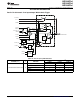
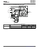
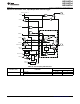

Direction
0: Input
1: Output
P1SEL.x
P1DIR.x
P1IN.x
P1IRQ.x
D
EN
To Timer_A3
From Timer_A3
P1OUT.x
Interrupt
Edge Select
Q
EN
Set
P1SEL.x
P1IES.x
P1IFG.x
P1IE.x
DVSS
DVCC
P1REN.x
Pad Logic
1
1
0
0
1
1
0
P1.1/TA1/SDCLK
P1.2/TA0/SD0DO
1
0
From SD24_A
P1SEL2.x
Bus
Keeper
EN
MSP430AFE2x3
MSP430AFE2x2
MSP430AFE2x1
SLAS701A – NOVEMBER 2010– REVISED MARCH 2011
www.ti.com
Port P1 Pin Schematic: P1.1 and P1.2 Input/Output With Schmitt Trigger
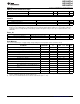
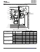
Table 18. Port P1 (P1.1 and P1.2) Pin Functions
CONTROL BITS / SIGNAL
(1)
PIN NAME (P1.x) x FUNCTION
P1DIR.x P1SEL.x P1SEL2.x
P1.1 (I/O) I: 0, O: 1 0 X
Timer_A3.CCI1A and CCI1B 0 1 0
P1.1/TA1/SDCLK 1
Timer_A3.TA1 1 1 0
SDCLK 1 1 1
P1.2 (I/O) I: 0, O: 1 0 X
Timer_A3.CCI0A and CCI0B 0 1 0
P1.2/TA0/SD0DO 2
Timer_A3.TA0 1 1 0
SD0DO 1 1 1
(1) X = don't care
34 Submit Documentation Feedback Copyright © 2010–2011, Texas Instruments Incorporated