
Datasheet


MSP430AFE2x3
MSP430AFE2x2
MSP430AFE2x1
www.ti.com
SLAS701A –NOVEMBER 2010–REVISED MARCH 2011
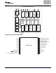
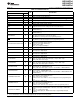
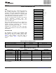
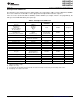
Table 2. Terminal Functions
TERMINAL
I/O DESCRIPTION
NAME NO.
A0.0+ 1 I SD24_A positive analog input A0.0
(1)
A0.0- 2 I SD24_A negative analog input A0.0
(1)
A1.0+ 3 I SD24_A positive analog input A1.0 (not available on MSP430AFE2x1)
(1)
A1.0- 4 I SD24_A negative analog input A1.0 (not available on MSP430AFE2x1)
(1)
AVCC 5 Analog supply voltage, positive terminal. Must not power up prior to DVCC.
AVSS 6 Analog supply voltage, negative terminal
Input for an external reference voltage/
VREF 7 I/O
output for internal reference voltage (can be used as mid-voltage)
SD24_A positive analog input A2.0 (not available on MSP430AFE2x2 and
A2.0+ 8 I
MSP430AFE2x1)
(1)
SD24_A negative analog input A2.0 (not available on MSP430AFE2x2 and
A2.0- 9 I
MSP430AFE2x1)
(1)
Selects test mode for JTAG pins on P1.5 to P1.7 and P2.0.
TEST/SBWTCK 10 I The device protection fuse is connected to TEST.
Spy-Bi-Wire test clock input for device programming and test.
Reset or nonmaskable interrupt input
RST/NMI/SBWTDIO 11 I
Spy-Bi-Wire test data input/output for device programming and test.
General-purpose digital I/O pin
Analog input to supply voltage supervisor
P1.0/SVSIN/TACLK/SMCLK/TA2 12 I/O Timer_A3, clock signal TACLK input
SMCLK signal output
Timer_A3, compare: Out2 Output
DVSS 13 Digital supply voltage, negative terminal
Input terminal of crystal oscillator
P2.6/XT2IN 14 I/O
General-purpose digital I/O pin
Output terminal of crystal oscillator
P2.7/XT2OUT 15 I/O
General-purpose digital I/O pin
DVCC 16 Digital supply voltage, positive terminal.
General-purpose digital I/O pin
P1.1/TA1/SDCLK 17 I/O Timer_A3, capture: CCI1A and CCI1B inputs, compare: Out1 output
SD24_A bit stream clock output
General-purpose digital I/O pin
P1.2/TA0/SD0DO 18 I/O Timer_A3, capture: CCI0A and CCI0B inputs, compare: Out0 output
SD24_A bit stream data output for channel 0
General-purpose digital I/O pin
P1.3/UTXD0/SD1DO 19 I/O Transmit data out - USART0/UART mode
SD24_A bit stream data output for channel 1 (not available on MSP430AFE2x1)
General-purpose digital I/O pin
Receive data in - USART0/UART mode
P1.4/URXD0/SD2DO 20 I/O
SD24_A bit stream data output for channel 2 (not available on MSP430AFE2x2 and
MSP430AFE2x1)
General-purpose digital I/O
Slave in/master out of USART0/SPI mode
P1.5/SIMO0/SVSOUT/TMS 21 I/O SVS: output of SVS comparator
JTAG test mode select. TMS is used as an input port for device programming and
test.
General-purpose digital I/O pin
Slave out/master in of USART0/SPI mode
P1.6/SOMI0/TA2/TCK 22 I/O
Timer_A3, compare: Out2 output
JTAG test clock. TCK is the clock input port for device programming and test.
General-purpose digital I/O pin
External clock input - USART0/UART or SPI mode, clock output - USART0/SPI
mode.
P1.7/UCLK0/TA1/TDO/TDI 23 I/O
Timer_A3, compare: Out1 output
JTAG test data output port. TDO/TDI data output or programming data input
terminal.
(1) It is recommended to short unused analog input pairs and connect them to analog ground.
Copyright © 2010–2011, Texas Instruments Incorporated Submit Documentation Feedback 5