
Datasheet


MSP430BT5190
www.ti.com
SLAS703A –APRIL 2010–REVISED AUGUST 2013
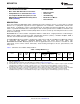
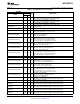
Table 2. Terminal Functions (continued)
TERMINAL
NO. I/O
(1)
DESCRIPTION
NAME
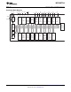
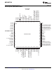
PZ ZQW
General-purpose digital I/O with port interrupt
P2.1/TA1.0 26 L2 I/O
TA1 CCR0 capture: CCI0A input, compare: Out0 output
General-purpose digital I/O with port interrupt
P2.2/TA1.1 27 M2 I/O
TA1 CCR1 capture: CCI1A input, compare: Out1 output
General-purpose digital I/O with port interrupt
P2.3/TA1.2 28 L3 I/O
TA1 CCR2 capture: CCI2A input, compare: Out2 output
General-purpose digital I/O with port interrupt
P2.4/RTCCLK 29 M3 I/O
RTCCLK output
P2.5 30 L4 I/O General-purpose digital I/O with port interrupt
General-purpose digital I/O with port interrupt
P2.6/ACLK 31 M4 I/O
ACLK output (divided by 1, 2, 4, 8, 16, or 32)
General-purpose digital I/O with port interrupt
P2.7/ADC12CLK/DMAE0 32 J5 I/O Conversion clock output ADC
DMA external trigger input
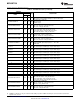
General-purpose digital I/O
Slave transmit enable – USCI_B0 SPI mode
P3.0/UCB0STE/UCA0CLK 33 L5 I/O
Clock signal input – USCI_A0 SPI slave mode
Clock signal output – USCI_A0 SPI master mode
General-purpose digital I/O
P3.1/UCB0SIMO/UCB0SDA 34 M5 I/O Slave in, master out – USCI_B0 SPI mode
I2C data – USCI_B0 I2C mode
General-purpose digital I/O
P3.2/UCB0SOMI/UCB0SCL 35 J6 I/O Slave out, master in – USCI_B0 SPI mode
I2C clock – USCI_B0 I2C mode
General-purpose digital I/O
Clock signal input – USCI_B0 SPI slave mode
P3.3/UCB0CLK/UCA0STE 36 L6 I/O
Clock signal output – USCI_B0 SPI master mode
Slave transmit enable – USCI_A0 SPI mode
DVSS3 37 M6 Digital ground supply
DVCC3 38 M7 Digital power supply
General-purpose digital I/O
P3.4/UCA0TXD/UCA0SIMO 39 L7 I/O Transmit data – USCI_A0 UART mode
Slave in, master out – USCI_A0 SPI mode
General-purpose digital I/O
P3.5/UCA0RXD/UCA0SOMI 40 J7 I/O Receive data – USCI_A0 UART mode
Slave out, master in – USCI_A0 SPI mode
General-purpose digital I/O
Slave transmit enable – USCI_B1 SPI mode
P3.6/UCB1STE/UCA1CLK 41 M8 I/O
Clock signal input – USCI_A1 SPI slave mode
Clock signal output – USCI_A1 SPI master mode
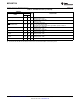
General-purpose digital I/O
P3.7/UCB1SIMO/UCB1SDA 42 L8 I/O Slave in, master out – USCI_B1 SPI mode
I2C data – USCI_B1 I2C mode
General-purpose digital I/O
P4.0/TB0.0 43 J8 I/O
TB0 capture CCR0: CCI0A/CCI0B input, compare: Out0 output
General-purpose digital I/O
P4.1/TB0.1 44 M9 I/O
TB0 capture CCR1: CCI1A/CCI1B input, compare: Out1 output
General-purpose digital I/O
P4.2/TB0.2 45 L9 I/O
TB0 capture CCR2: CCI2A/CCI2B input, compare: Out2 output
General-purpose digital I/O
P4.3/TB0.3 46 L10 I/O
TB0 capture CCR3: CCI3A/CCI3B input, compare: Out3 output
General-purpose digital I/O
P4.4/TB0.4 47 M10 I/O
TB0 capture CCR4: CCI4A/CCI4B input, compare: Out4 output
General-purpose digital I/O
P4.5/TB0.5 48 L11 I/O
TB0 capture CCR5: CCI5A/CCI5B input, compare: Out5 output
Copyright © 2010–2013, Texas Instruments Incorporated Submit Documentation Feedback 7
Product Folder Links: MSP430BT5190