
Datasheet


MSP430BT5190
SLAS703A –APRIL 2010–REVISED AUGUST 2013
www.ti.com
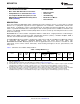
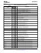
Table 2. Terminal Functions (continued)
TERMINAL
NO. I/O
(1)
DESCRIPTION
NAME
PZ ZQW
General-purpose digital I/O
P4.6/TB0.6 49 M11 I/O
TB0 capture CCR6: CCI6A/CCI6B input, compare: Out6 output
General-purpose digital I/O
P4.7/TB0CLK/SMCLK 50 M12 I/O TB0 clock input
SMCLK output
General-purpose digital I/O
P5.4/UCB1SOMI/UCB1SCL 51 L12 I/O Slave out, master in – USCI_B1 SPI mode
I2C clock – USCI_B1 I2C mode
General-purpose digital I/O
Clock signal input – USCI_B1 SPI slave mode
P5.5/UCB1CLK/UCA1STE 52 J9 I/O
Clock signal output – USCI_B1 SPI master mode
Slave transmit enable – USCI_A1 SPI mode
General-purpose digital I/O
P5.6/UCA1TXD/UCA1SIMO 53 K11 I/O Transmit data – USCI_A1 UART mode
Slave in, master out – USCI_A1 SPI mode
General-purpose digital I/O
P5.7/UCA1RXD/UCA1SOMI 54 K12 I/O Receive data – USCI_A1 UART mode
Slave out, master in – USCI_A1 SPI mode
General-purpose digital I/O
P7.2/TB0OUTH/SVMOUT 55 J11 I/O Switch all PWM outputs high impedance – Timer TB0
SVM output
General-purpose digital I/O
P7.3/TA1.2 56 J12 I/O
TA1 CCR2 capture: CCI2B input, compare: Out2 output
General-purpose digital I/O
P8.0/TA0.0 57 H9 I/O
TA0 CCR0 capture: CCI0B input, compare: Out0 output
General-purpose digital I/O
P8.1/TA0.1 58 H11 I/O
TA0 CCR1 capture: CCI1B input, compare: Out1 output
General-purpose digital I/O
P8.2/TA0.2 59 H12 I/O
TA0 CCR2 capture: CCI2B input, compare: Out2 output
General-purpose digital I/O
P8.3/TA0.3 60 G9 I/O
TA0 CCR3 capture: CCI3B input, compare: Out3 output
General-purpose digital I/O
P8.4/TA0.4 61 G11 I/O
TA0 CCR4 capture: CCI4B input, compare: Out4 output
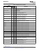
VCORE
(2)
62 G12 Regulated core power supply output (internal use only, no external current loading)
DVSS2 63 F12 Digital ground supply
DVCC2 64 E12 Digital power supply
General-purpose digital I/O
P8.5/TA1.0 65 F11 I/O
TA1 CCR0 capture: CCI0B input, compare: Out0 output
General-purpose digital I/O
P8.6/TA1.1 66 E11 I/O
TA1 CCR1 capture: CCI1B input, compare: Out1 output
P8.7 67 D12 I/O General-purpose digital I/O
General-purpose digital I/O
Slave transmit enable – USCI_B2 SPI mode
P9.0/UCB2STE/UCA2CLK 68 D11 I/O
Clock signal input – USCI_A2 SPI slave mode
Clock signal output – USCI_A2 SPI master mode
General-purpose digital I/O
P9.1/UCB2SIMO/UCB2SDA 69 F9 I/O Slave in, master out – USCI_B2 SPI mode
I2C data – USCI_B2 I2C mode
General-purpose digital I/O
P9.2/UCB2SOMI/UCB2SCL 70 C12 I/O Slave out, master in – USCI_B2 SPI mode
I2C clock – USCI_B2 I2C mode
(2) VCORE is for internal use only. No external current loading is possible. VCORE should only be connected to the recommended
capacitor value, C
VCORE
.
8 Submit Documentation Feedback Copyright © 2010–2013, Texas Instruments Incorporated
Product Folder Links: MSP430BT5190