
Datasheet


MSP430BT5190
SLAS703A –APRIL 2010–REVISED AUGUST 2013
www.ti.com
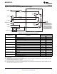
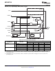
Table 48. Port P5 (P5.0 and P5.1) Pin Functions
CONTROL BITS/SIGNALS
(1)
PIN NAME (P5.x) x FUNCTION
P5DIR.x P5SEL.x REFOUT
P5.0/A8/VREF+/VeREF+ 0 P5.0 (I/O)
(2)
I: 0; O: 1 0 X
A8/VeREF+
(3)
X 1 0
A8/VREF+
(4)
X 1 1
P5.1/A9/VREF–/VeREF– 1 P5.1 (I/O)
(2)
I: 0; O: 1 0 X
A9/VeREF–
(5)
X 1 0
A9/VREF–
(6)
X 1 1
(1) X = Don't care
(2) Default condition
(3) Setting the P5SEL.0 bit disables the output driver as well as the input Schmitt trigger to prevent parasitic cross currents when applying
analog signals. An external voltage can be applied to VeREF+ and used as the reference for the ADC12_A. Channel A8, when selected
with the INCHx bits, is connected to the VREF+/VeREF+ pin.
(4) Setting the P5SEL.0 bit disables the output driver as well as the input Schmitt trigger to prevent parasitic cross currents when applying
analog signals. The ADC12_A, VREF+ reference is available at the pin. Channel A8, when selected with the INCHx bits, is connected to
the VREF+/VeREF+ pin.
(5) Setting the P5SEL.1 bit disables the output driver as well as the input Schmitt trigger to prevent parasitic cross currents when applying
analog signals. An external voltage can be applied to VeREF- and used as the reference for the ADC12_A. Channel A9, when selected
with the INCHx bits, is connected to the VREF-/VeREF- pin.
(6) Setting the P5SEL.1 bit disables the output driver as well as the input Schmitt trigger to prevent parasitic cross currents when applying
analog signals. The ADC12_A, VREF– reference is available at the pin. Channel A9, when selected with the INCHx bits, is connected to
the VREF-/VeREF- pin.
76 Submit Documentation Feedback Copyright © 2010–2013, Texas Instruments Incorporated
Product Folder Links: MSP430BT5190