
Datasheet

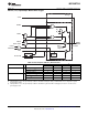


P7.2/TB0OUTH/SVMOUT
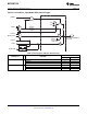
P7.3/TA1.2
Direction
0: Input
1: Output
P7SEL.x
1
0
P7DIR.x
P7IN.x
EN
Module X IN
1
0
Module X OUT
P7OUT.x
1
0
DV
SS
DV
CC
P7REN.x
Pad Logic
1
P7DS.x
0: Low drive
1: High drive
D
MSP430BT5190
SLAS703A –APRIL 2010–REVISED AUGUST 2013
www.ti.com
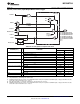
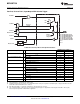
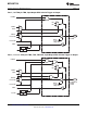
Port P7, P7.2 and P7.3, Input/Output With Schmitt Trigger
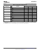
Table 53. Port P7 (P7.2 and P7.3) Pin Functions
CONTROL BITS/SIGNALS
PIN NAME (P7.x) x FUNCTION
P7DIR.x P7SEL.x
P7.2/TB0OUTH/SVMOUT 2 P7.2 (I/O) I: 0; O: 1 0
TB0OUTH 0 1
SVMOUT 1 1
P7.3/TA1.2 3 P7.3 (I/O) I: 0; O: 1 0
TA1.CCI2B 0 1
TA1.2 1 1
84 Submit Documentation Feedback Copyright © 2010–2013, Texas Instruments Incorporated
Product Folder Links: MSP430BT5190