
Datasheet

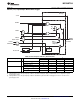
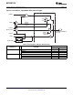

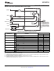
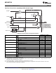

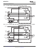

P9.0/UCB2STE/UCA2CLK
P9.1/UCB2SIMO/UCB2SDA
P9.2/UCB2SOMI/UCB2SCL
P9.3/UCB2CLK/UCA2STE
P9.4/UCA2TXD/UCA2SIMO
P9.5/UCA2RXD/UCA2SOMI
P9.6
P9.7
Direction
0: Input
1: Output
P9SEL.x
1
0
P9DIR.x
P9IN.x
EN
Module X IN
1
0
Module X OUT
P9OUT.x
1
0
DV
SS
DV
CC
P9REN.x
Pad Logic
1
P9DS.x
0: Low drive
1: High drive
D
MSP430BT5190
www.ti.com
SLAS703A –APRIL 2010–REVISED AUGUST 2013
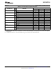
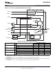
Port P9, P9.0 to P9.7, Input/Output With Schmitt Trigger
Table 56. Port P9 (P9.0 to P9.7) Pin Functions
CONTROL BITS/SIGNALS
(1)
PIN NAME (P9.x) x FUNCTION
P9DIR.x P9SEL.x
P9.0/UCB2STE/UCA2CLK 0 P9.0 (I/O) I: 0; O: 1 0
UCB2STE/UCA2CLK
(2) (3)
X 1
P9.1/UCB2SIMO/UCB2SDA 1 P9.1 (I/O) I: 0; O: 1 0
UCB2SIMO/UCB2SDA
(2) (4)
X 1
P9.2/UCB2SOMI/UCB2SCL 2 P9.2 (I/O) I: 0; O: 1 0
UCB2SOMI/UCB2SCL
(2) (4)
X 1
P9.3/UCB2CLK/UCA2STE 3 P9.3 (I/O) I: 0; O: 1 0
UCB2CLK/UCA2STE
(2)(5)
X 1
P9.4/UCA2TXD/UCA2SIMO 4 P9.4 (I/O) I: 0; O: 1 0
UCA2TXD/UCA2SIMO
(2)
X 1
P9.5/UCA2RXD/UCA2SOMI 5 P9.5 (I/O) I: 0; O: 1 0
UCA2RXD/UCA2SOMI
(2)
X 1
P9.6 6 P9.6 (I/O) I: 0; O: 1 0
P9.7 7 P9.7 (I/O) I: 0; O: 1 0
(1) X = Don't care
(2) The pin direction is controlled by the USCI module.
(3) UCA2CLK function takes precedence over UCB2STE function. If the pin is required as UCA2CLK input or output, USCI B2 is forced to
3-wire SPI mode if 4-wire SPI mode is selected.
(4) If the I2C functionality is selected, the output drives only the logical 0 to V
SS
level.
(5) UCB2CLK function takes precedence over UCA2STE function. If the pin is required as UCB2CLK input or output, USCI A2 is forced to
3-wire SPI mode if 4-wire SPI mode is selected.
Copyright © 2010–2013, Texas Instruments Incorporated Submit Documentation Feedback 87
Product Folder Links: MSP430BT5190