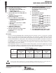
SLAS439A − SEPTEMBER 2004 − REVISED JUNE 2005 D Low Supply Voltage Range 1.8 V to 3.6 V D Ultralow-Power Consumption D D D D D D D Serial Onboard Programming, − Active Mode: 250 µA at 1 MHz, 2.2 V − Standby Mode: 0.7 µA − Off Mode (RAM Retention): 0.
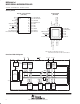
SLAS439A − SEPTEMBER 2004 − REVISED JUNE 2005 device pinout 19 P1.6/TA1/TDI/TCLK 3 18 P1.5/TA0/TMS VSS XOUT/P2.7/CA7 4 17 5 16 P1.4/SMCLK/TCK P1.3/TA2 XIN/P2.6/CA6 6 15 P1.2/TA1 RST/NMI P2.0/ACLK/CA2 P2.1/INCLK/CA3 7 14 8 13 9 12 P1.1/TA0 P1.0/TACLK P2.4/TA2/CA1 10 11 P2.3/TA1/CA0 24 23 22 21 20 19 1 VSS 2 XOUT/P2.7/CA7 3 XIN/P2.6/CA6 4 18 P1.5/TA0/TMS 17 P1.4/SMCLK/TCK 16 P1.3/TA2 15 P1.2/TA1 14 P1.1/TA0 13 P1.0/TACLK 5 6 NC P2.
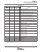
SLAS439A − SEPTEMBER 2004 − REVISED JUNE 2005 Terminal Functions TERMINAL DW, PW, or DGV RGE NO. NO. P1.0/TACLK 13 13 I/O General-purpose digital I/O pin Timer_A, clock signal TACLK input P1.1/TA0 14 14 I/O General-purpose digital I/O pin Timer_A, capture: CCI0A input, compare: Out0 output/BSL transmit P1.2/TA1 15 15 I/O General-purpose digital I/O pin Timer_A, capture: CCI1A input, compare: Out1 output P1.
SLAS439A − SEPTEMBER 2004 − REVISED JUNE 2005 short-form description CPU The MSP430 CPU has a 16-bit RISC architecture that is highly transparent to the application. All operations, other than program-flow instructions, are performed as register operations in conjunction with seven addressing modes for source operand and four addressing modes for destination operand.
SLAS439A − SEPTEMBER 2004 − REVISED JUNE 2005 operating modes The MSP430 has one active mode and five software selectable low-power modes of operation. An interrupt event can wake up the device from any of the five low-power modes, service the request and restore back to the low-power mode on return from the interrupt program.
SLAS439A − SEPTEMBER 2004 − REVISED JUNE 2005 interrupt vector addresses The interrupt vectors and the power-up starting address are located in the address range of 0FFFFh−0FFC0h. The vector contains the 16-bit address of the appropriate interrupt handler instruction sequence. If the reset vector (located at address 0FFFEh) contains 0FFFFh (e.g. flash is not programmed) the CPU will go into LPM4 immediately after power−up.
SLAS439A − SEPTEMBER 2004 − REVISED JUNE 2005 special function registers Most interrupt and module enable bits are collected into the lowest address space. Special function register bits not allocated to a functional purpose are not physically present in the device. Simple software access is provided with this arrangement.
SLAS439A − SEPTEMBER 2004 − REVISED JUNE 2005 memory organization MSP430F2101 MSP430F2111 MSP430F2121 MSP430F2131 Memory Main: interrupt vector Main: code memory Size Flash Flash 1KB Flash 0FFFFh−0FFE0h 0FFFFh−0FC00h 2KB Flash 0FFFFh−0FFE0h 0FFFFh−0F800h 4KB Flash 0FFFFh−0FFE0h 0FFFFh−0F000h 8KB Flash 0FFFFh−0FFE0h 0FFFFh−0E000h Information memory Size Flash 256 Byte 010FFh − 01000h 256 Byte 010FFh − 01000h 256 Byte 010FFh − 01000h 256 Byte 010FFh − 01000h
SLAS439A − SEPTEMBER 2004 − REVISED JUNE 2005 peripherals Peripherals are connected to the CPU through data, address, and control busses and can be handled using all instructions. For complete module descriptions, refer to the MSP430x2xx Family User’s Guide.
SLAS439A − SEPTEMBER 2004 − REVISED JUNE 2005 comparator_A+ The primary function of the Comparator_A+ module is to support precision slope analog-to-digital conversions, battery-voltage supervision, and monitoring of external analog signals. timer_A3 Timer_A3 is a 16-bit timer/counter with three capture/compare registers. Timer_A3 can support multiple capture/compares, PWM outputs, and interval timing. Timer_A3 also has extensive interrupt capabilities.
SLAS439A − SEPTEMBER 2004 − REVISED JUNE 2005 peripheral file map PERIPHERALS WITH WORD ACCESS Timer_A Capture/compare register Capture/compare register Capture/compare register Timer_A register Capture/compare control Capture/compare control Capture/compare control Timer_A control Timer_A interrupt vector TACCR2 TACCR1 TACCR0 TAR TACCTL2 TACCTL1 TACCTL0 TACTL TAIV 0176h 0174h 0172h 0170h 0166h 0164h 0162h 0160h 012Eh Flash Memory Flash control 3 Flash control 2 F
SLAS439A − SEPTEMBER 2004 − REVISED JUNE 2005 absolute maximum ratings (see Note 1) Voltage applied at VCC to VSS . . . . . . . . . . . . . . . . . . . . . . . . . . . . . . . . . . . . . . . . . . . . . . . . . . . . . . −0.3 V to 4.1 V Voltage applied to any pin (see Note 2) . . . . . . . . . . . . . . . . . . . . . . . . . . . . . . . . . . . . . . . . . −0.3 V to VCC+0.3 V Diode current at any device terminal . . . . . . . . . . . . . . . . . . . . . . . . . . . . .
SLAS439A − SEPTEMBER 2004 − REVISED JUNE 2005 electrical characteristics over recommended ranges of supply voltage and operating free-air temperature (unless otherwise noted) active mode supply current (into VCC) excluding external current (see Notes 1 and 2) PARAMETER IAM, 1MHz IAM, 1MHz IAM, 4kHz IAM,100kHz TEST CONDITIONS Active mode (AM) current (1MHz) Active mode (AM) current (1MHz) Active mode (AM) current (4kHz) Active mode (AM) current (100kHz) VCC f
SLAS439A − SEPTEMBER 2004 − REVISED JUNE 2005 electrical characteristics over recommended ranges of supply voltage and operating free-air temperature (unless otherwise noted) low power mode supply currents (into VCC) excluding external current (see Notes 1 and 2) PARAMETER TEST CONDITIONS VCC Low-power mode 0 (LPM0) current, see Note 3 fMCLK = 0MHz, fSMCLK = fDCO = 1MHz, fACLK = 32,768Hz, BCSCTL1 = CALBC1_1MHz, DCOCTL = CALDCO_1MHz, CPUOFF = 1, SCG0 = 0, SCG1 = 0, OS
SLAS439A − SEPTEMBER 2004 − REVISED JUNE 2005 electrical characteristics over recommended ranges of supply voltage and operating free-air temperature (unless otherwise noted) (continued) Schmitt-trigger inputs − Ports P1 and P2 PARAMETER VIT+ VIT− TEST CONDITIONS Positive-going input threshold voltage Negative-going input threshold voltage Vhys Input voltage hysteresis (VIT+ − VIT−) RPull Pull−up/pull−down resistor For pull−up: VIN = VSS; For pull−down: VIN =
SLAS439A − SEPTEMBER 2004 − REVISED JUNE 2005 electrical characteristics over recommended ranges of supply voltage and operating free-air temperature (unless otherwise noted) (continued) outputs − Ports P1 and P2 PARAMETER IL Maximum load current per port pin ILT Maximum combined load current (all port pins) VOH VOL High-level output voltage Low-level output voltage TEST CONDITIONS VCC I(OHmax) = −1.
SLAS439A − SEPTEMBER 2004 − REVISED JUNE 2005 electrical characteristics over recommended ranges of supply voltage and operating free-air temperature (unless otherwise noted) (continued) typical characteristics − outputs TYPICAL LOW-LEVEL OUTPUT CURRENT vs LOW-LEVEL OUTPUT VOLTAGE TYPICAL LOW-LEVEL OUTPUT CURRENT vs LOW-LEVEL OUTPUT VOLTAGE 50.0 I OL − Typical Low-Level Output Current − mA I OL − Typical Low-Level Output Current − mA 25.0 TA = 25°C VCC = 2.2 V P2.
SLAS439A − SEPTEMBER 2004 − REVISED JUNE 2005 electrical characteristics over recommended ranges of supply voltage and operating free-air temperature (unless otherwise noted) (continued) POR/brownout reset (BOR) (see Notes 1 and 2) PARAMETER TEST CONDITIONS VCC(start) (see Figure 8) dVCC/dt ≤ 3 V/s V(B_IT−) Vhys(B_IT−) (see Figure 8 through Figure 10) dVCC/dt ≤ 3 V/s dVCC/dt ≤ 3 V/s td(BOR) (see Figure 8) t(reset) Pulse length needed at RST/NMI pin to accepte
SLAS439A − SEPTEMBER 2004 − REVISED JUNE 2005 electrical characteristics over recommended ranges of supply voltage and operating free-air temperature (unless otherwise noted) (continued) typical characteristics − POR/brownout reset (BOR) VCC 3V 2 VCC(min)− V VCC = 3 V Typical Conditions t pw 1.5 1 VCC(min) 0.5 0 0.001 1 1000 1 ns tpw − Pulse Width − µs 1 ns tpw − Pulse Width − µs Figure 9.
SLAS439A − SEPTEMBER 2004 − REVISED JUNE 2005 electrical characteristics over recommended ranges of supply voltage and operating free-air temperature (unless otherwise noted) (continued) main DCO characteristics D All ranges selected by RSELx overlap with RSELx + 1: RSELx = 0 overlaps RSELx = 1, ... RSELx = 14 overlaps RSELx = 15. D DCO control bits DCOx have a step size as defined by parameter SDCO.
SLAS439A − SEPTEMBER 2004 − REVISED JUNE 2005 electrical characteristics over recommended ranges of supply voltage and operating free-air temperature (unless otherwise noted) (continued) calibrated DCO frequencies − tolerance at calibration PARAMETER TEST CONDITIONS Frequency tolerance at calibration TA 25°C VCC MIN TYP MAX UNIT 3V −1 ±0.2 +1 25°C 3V 0.990 1 1.
SLAS439A − SEPTEMBER 2004 − REVISED JUNE 2005 electrical characteristics over recommended ranges of supply voltage and operating free-air temperature (unless otherwise noted) (continued) calibrated DCO frequencies − tolerance over supply voltage VCC PARAMETER TEST CONDITIONS 1 MHz tolerance over VCC TA 25°C VCC MIN TYP MAX UNIT 1.8 V − 3.6 V −2.5 ±2 +2.5 % 8 MHz tolerance over VCC 25°C 1.8 V − 3.6 V −2.5 ±2 +2.5 % 12 MHz tolerance over VCC 25°C 2.
SLAS439A − SEPTEMBER 2004 − REVISED JUNE 2005 typical characteristics − calibrated 1MHz DCO frequency 1.03 1.02 VCC = 1.8 V Frequency − MHz 1.01 VCC = 2.2 V 1.00 VCC = 3.0 V 0.99 VCC = 3.6 V 0.98 0.97 −50.0 −25.0 0.0 25.0 50.0 75.0 100.0 TA − Temperature − °C Figure 11. Calibrated 1 MHz Frequency vs. Temperature 1.03 Frequency − MHz 1.02 1.01 TA = 105 °C 1.00 TA = 85 °C TA = 25 °C 0.99 TA = −40 °C 0.98 0.97 1.5 2.0 2.5 3.0 3.5 4.
SLAS439A − SEPTEMBER 2004 − REVISED JUNE 2005 electrical characteristics over recommended ranges of supply voltage and operating free-air temperature (unless otherwise noted) (continued) wake-up from lower power modes (LPM3/4) PARAMETER TEST CONDITIONS DCO clock wake−up time from tDCO,LPM3/4 LPM3/4 (see Note 1) VCC MIN TYP MAX BCSCTL1= CALBC1_1MHz; DCOCTL = CALDCO_1MHz 2.2 V/3 V 2 BCSCTL1= CALBC1_8MHz; DCOCTL = CALDCO_8MHz 2.2 V/3 V 1.
SLAS439A − SEPTEMBER 2004 − REVISED JUNE 2005 electrical characteristics over recommended ranges of supply voltage and operating free-air temperature (unless otherwise noted) (continued) crystal oscillator, LFXT1, low frequency modes (see Note 4) PARAMETER fLFXT1,LF LFXT1 oscillator crystal frequency, LF mode 0, 1 LFXT1 oscillator logic level fLFXT1,LF,logic square wave input frequency, LF mode OALF CL,eff Oscillation Allowance for LF crystals Integrated effectiv
SLAS439A − SEPTEMBER 2004 − REVISED JUNE 2005 electrical characteristics over recommended ranges of supply voltage and operating free-air temperature (unless otherwise noted) (continued) crystal oscillator, LFXT1, high frequency modes (see Note 5) PARAMETER TEST CONDITIONS VCC MIN TYP MAX UNIT fLFXT1,HF0 LFXT1 oscillator crystal frequency, HF mode 0 XTS = 1, LFXT1Sx = 0 1.8 V − 3.6 V 0.
SLAS439A − SEPTEMBER 2004 − REVISED JUNE 2005 electrical characteristics over recommended ranges of supply voltage and operating free-air temperature (unless otherwise noted) (continued) typical characteristics − LFXT1 oscillator in HF mode (XTS = 1) Oscillation Allowance − Ohms 100000.00 10000.00 1000.00 LFXT1Sx = 3 100.00 LFXT1Sx = 2 LFXT1Sx = 1 10.00 0.10 1.00 10.00 100.00 Crystal Frequency − MHz Figure 14.
SLAS439A − SEPTEMBER 2004 − REVISED JUNE 2005 electrical characteristics over recommended ranges of supply voltage and operating free-air temperature (unless otherwise noted) (continued) Timer_A PARAMETER TEST CONDITIONS fTA Timer_A clock frequency tTA,cap Timer_A, capture timing Internal: SMCLK, ACLK; External: TACLK, INCLK; Duty Cycle = 50% ±10% TA0, TA1, TA2 VCC MIN TYP MAX 2.2 V 10 3V 16 UNIT MHz 2.
SLAS439A − SEPTEMBER 2004 − REVISED JUNE 2005 electrical characteristics over recommended ranges of supply voltage and operating free-air temperature (unless otherwise noted) (continued) 0 V VCC 0 1 CAF CAON To Internal Modules Low Pass Filter + _ V+ V− 0 0 1 1 CAOUT Set CAIFG Flag τ ≈ 2.0 µs Figure 16. Block Diagram of Comparator_A+ Module VCAOUT Overdrive V− 400 mV t(response) V+ Figure 17.
SLAS439A − SEPTEMBER 2004 − REVISED JUNE 2005 electrical characteristics over recommended ranges of supply voltage and operating free-air temperature (unless otherwise noted) (continued) typical characteristics − Comparator_A+ 650 650 VCC = 2.2 V V(REFVT) − Reference Volts −mV V(REFVT) − Reference Volts −mV VCC = 3 V 600 Typical 550 500 450 400 −45 −25 −5 15 35 55 75 600 Typical 550 500 450 400 −45 95 −25 −5 15 Short Resistance − kOhms 100.
SLAS439A − SEPTEMBER 2004 − REVISED JUNE 2005 electrical characteristics over recommended ranges of supply voltage and operating free-air temperature (unless otherwise noted) (continued) Flash Memory PARAMETER VCC(PGM/ ERASE) TEST CONDITIONS VCC Program and Erase supply voltage MIN TYP 2.2 257 MAX UNIT 3.6 V fFTG IPGM Flash Timing Generator frequency 476 kHz Supply current from VCC during program 2.2 V/3.
SLAS439A − SEPTEMBER 2004 − REVISED JUNE 2005 APPLICATION INFORMATION Port P1 pin schematic: P1.0 to P1.3, input/output with Schmitt-trigger Pad Logic P1REN.x P1DIR.x 0 0 Module X OUT 1 0 1 1 Direction 0: Input 1: Output 1 P1OUT.x DVSS DVCC P1.0/TACLK P1.1/TA0 P1.2/TA1 P1.3/TA2 P1SEL.x P1IN.x EN Module X IN D P1IE.x EN P1IRQ.x Q Set P1IFG.x Interrupt Edge Select P1SEL.x P1IES.x Port P1 (P1.0 to P1.3) pin functions PIN NAME (P1.X) P1.
SLAS439A − SEPTEMBER 2004 − REVISED JUNE 2005 Port P1 pin schematic: P1.4 to P1.7, input/output with Schmitt-trigger and in-system access features Pad Logic P1REN.1 P1DIR.1 0 P1OUT.1 0 1 0 1 1 Direction 0: Input 1: Output 1 Module X OUT DVSS DVCC P1.4/SMCLK/TCK P1.5/TA0/TMS P1.6/TA1/TDI P1.7/TA2/TDO/TDI Bus Keeper P1SEL.1 EN P1IN.1 EN Module X IN D P1IE.1 P1IRQ.1 EN Q P1IFG.1 P1SEL.1 P1IES.
SLAS439A − SEPTEMBER 2004 − REVISED JUNE 2005 Port P1 (P1.4 to P1.7) pin functions PIN NAME (P1.X) P1.4/SMCLK/TCK P1.5/TA0/TMS P1.6/TA1/TDI/TCLK P1.7/TA2/TDO/TDI CONTROL BITS / SIGNALS X 4 5 6 7 FUNCTION P1.4† (I/O) P1SEL.x TEST I: 0; O: 1 0 0 SMCLK 1 1 0 TCK X X 1 I: 0; O: 1 0 0 P1.5† (I/O) Timer_A3.TA0 1 1 0 TMS X X 1 I: 0; O: 1 0 0 P1.6† (I/O) Timer_A3.TA1 1 1 0 TDI/TCLK (see Note 3) X X 1 I: 0; O: 1 0 0 P1.
SLAS439A − SEPTEMBER 2004 − REVISED JUNE 2005 Port P2 pin schematic: P2.0 to P2.5, input/output with Schmitt-trigger Pad Logic To Comparator _A From Comparator_A CAPD.x P2REN.x P2DIR.x 0 0 Module X OUT 1 0 1 1 Direction 0: Input 1: Output 1 P2OUT.x DVSS DVCC P2.0/ACLK/CA2 P2.1/INCLK/CA3 P2.2/CAOUT/TA0/CA4 P2.3/TA1/CA0 P2.4/TA2/CA1 P2.5/CA5 Bus Keeper P2SEL.x EN P2IN.x EN Module X IN D P2IE.x P2IRQ.x EN Q Set P2IFG.x P2SEL.x P2IES.
SLAS439A − SEPTEMBER 2004 − REVISED JUNE 2005 Port P2 (P2.0 to P2.5) pin functions PIN NAME (P2.X) P2.0/ACLK/CA2 P2.1/INCLK/CA3 P2.2/CAOUT/TA0/CA4 CONTROL BITS / SIGNALS X 0 1 2 FUNCTION P2.0† (I/O) 3 P2.5/CA5 5 0 1 1 0 X X 1 I: 0; O: 1 0 0 Timer_A3.INCLK 0 1 0 DVSS CA3 (see Note 3) 1 1 0 X X 1 P2.1† (I/O) P2.2† (I/O) I: 0; O: 1 0 0 Timer_A3.CCI0B 0 1 0 Comparator_A.OUT 1 1 0 P2.3† (I/O) CA0 (see Note 3) 4 CAPD.
SLAS439A − SEPTEMBER 2004 − REVISED JUNE 2005 Port P2 pin schematic: P2.6, input/output with Schmitt-trigger and crystal oscillator input Pad Logic To Comparator _A From Comparator_A CAPD.x LFXT1 Oscillator BCSCTL3.LFXT1Sx = 11 P2.7/XOUT/CA7 LFXT1 off 0 LFXT1CLK 1 P2REN.6 P2DIR.6 0 0 Module X OUT 1 0 DVCC 1 1 Direction 0: Input 1: Output 1 P2OUT.6 DVSS P2.6/XIN/CA6 Bus Keeper P2SEL.6 EN P2IN.6 EN Module X IN D P2IE.6 P2IRQ.6 EN Q Set P2IFG.
SLAS439A − SEPTEMBER 2004 − REVISED JUNE 2005 Port P2 pin schematic: P2.7, input/output with Schmitt-trigger and crystal oscillator output Pad Logic To Comparator _A From Comparator_A CAPD.x LFXT1 Oscillator BCSCTL3.LFXT1Sx = 11 LFXT1 off 0 LFXT1CLK P2.6/XIN/CA6 1 Pad Logic P2REN.7 P2DIR.7 0 0 Module X OUT 1 0 1 1 Direction 0: Input 1: Output 1 P2OUT.7 DVSS DVCC P2.7/XOUT/CA7 Bus Keeper P2SEL.7 EN P2IN.7 EN Module X IN D P2IE.7 P2IRQ.
SLAS439A − SEPTEMBER 2004 − REVISED JUNE 2005 Port P2 (P2.6) pin functions PIN NAME (P2.X) P2.6/XIN/CA6 CONTROL BITS / SIGNALS X 6 FUNCTION P2.6 (I/O) P2DIR.x P2SEL.x CAPD.x I: 0; O: 1 0 0 0 XIN† X 1 CA6 (see Note 3) X X 1 † Default after reset (PUC/POR) NOTES: 1. N/A: Not available or not applicable. 2. X: Don’t care. 3. Setting the CAPD.
SLAS439A − SEPTEMBER 2004 − REVISED JUNE 2005 JTAG fuse check mode MSP430 devices that have the fuse on the TEST terminal have a fuse check mode that tests the continuity of the fuse the first time the JTAG port is accessed after a power-on reset (POR). When activated, a fuse check current, ITF , of 1 mA at 3 V, 2.5 mA at 5 V can flow from the TEST pin to ground if the fuse is not burned.
PACKAGE OPTION ADDENDUM www.ti.
PACKAGE OPTION ADDENDUM www.ti.
MECHANICAL DATA MPDS006C – FEBRUARY 1996 – REVISED AUGUST 2000 DGV (R-PDSO-G**) PLASTIC SMALL-OUTLINE 24 PINS SHOWN 0,40 0,23 0,13 24 13 0,07 M 0,16 NOM 4,50 4,30 6,60 6,20 Gage Plane 0,25 0°– 8° 1 0,75 0,50 12 A Seating Plane 0,15 0,05 1,20 MAX PINS ** 0,08 14 16 20 24 38 48 56 A MAX 3,70 3,70 5,10 5,10 7,90 9,80 11,40 A MIN 3,50 3,50 4,90 4,90 7,70 9,60 11,20 DIM 4073251/E 08/00 NOTES: A. B. C. D. All linear dimensions are in millimeters.
MECHANICAL DATA MTSS001C – JANUARY 1995 – REVISED FEBRUARY 1999 PW (R-PDSO-G**) PLASTIC SMALL-OUTLINE PACKAGE 14 PINS SHOWN 0,30 0,19 0,65 14 0,10 M 8 0,15 NOM 4,50 4,30 6,60 6,20 Gage Plane 0,25 1 7 0°– 8° A 0,75 0,50 Seating Plane 0,15 0,05 1,20 MAX PINS ** 0,10 8 14 16 20 24 28 A MAX 3,10 5,10 5,10 6,60 7,90 9,80 A MIN 2,90 4,90 4,90 6,40 7,70 9,60 DIM 4040064/F 01/97 NOTES: A. B. C. D. All linear dimensions are in millimeters.
IMPORTANT NOTICE Texas Instruments Incorporated and its subsidiaries (TI) reserve the right to make corrections, modifications, enhancements, improvements, and other changes to its products and services at any time and to discontinue any product or service without notice. Customers should obtain the latest relevant information before placing orders and should verify that such information is current and complete.