MSP430F23x0 SLAS518E – AUGUST 2006 – REVISED AUGUST 2011 www.ti.com MIXED SIGNAL MICROCONTROLLER FEATURES 1 • • 2 • • • • • • Low Supply Voltage Range: 1.8 V to 3.6 V Ultra-Low Power Consumption – Active Mode: 270 µA at 1 MHz, 2.2 V – Standby Mode: 0.7 µA – Off Mode (RAM Retention): 0.1 µA Ultra-Fast Wake-Up From Standby Mode in Less Than 1 µs 16-Bit RISC Architecture, 62.
MSP430F23x0 SLAS518E – AUGUST 2006 – REVISED AUGUST 2011 www.ti.com This integrated circuit can be damaged by ESD. Texas Instruments recommends that all integrated circuits be handled with appropriate precautions. Failure to observe proper handling and installation procedures can cause damage. ESD damage can range from subtle performance degradation to complete device failure.
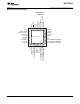
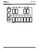
MSP430F23x0 SLAS518E – AUGUST 2006 – REVISED AUGUST 2011 www.ti.com Device Pinout, RHA Package 31 32 33 35 34 36 38 37 1 30 2 29 3 28 4 27 5 26 Exposed Thermal Pad 6 25 20 19 18 P4.4/TB1 P4.3/TB0 P4.2/TB2 P4.1/TB1 P4.0/TB0 P3.7 P3.6 P3.5/UCA0RXD/UCA0SOMI P3.4/UCA0TXD/UCA0SIMO P3.3/UCB0CLK/UCA0STE P1.7/TA2 P2.0/ACLK/CA2 P2.1/TAINCLK/CA3 P2.2/CAOUT/TA0/CA4 P2.3/CA0/TA1 P2.4/CA1/TA2 P2.5/ROSC/CA5 P3.0/UCB0STE/UCA0CLK P3.1/UCB0SIMO/UCB0SDA P3.
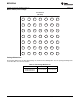
MSP430F23x0 SLAS518E – AUGUST 2006 – REVISED AUGUST 2011 www.ti.com Device Pinout, YFF Package YFF PACKAGE (TOP VIEW) A1 A2 A3 A4 A5 A6 A7 B1 B2 B3 B4 B5 B6 B7 C1 C2 C3 C4 C5 C6 C7 D1 D2 D3 D4 D5 D6 D7 E1 E2 E3 E4 E5 E6 E7 F1 F2 F3 F4 F5 F6 F7 G1 G2 G3 G4 G5 G6 G7 Package Dimensions The package dimensions for this YFF package are shown in the following table. See the package drawing at the end of this data sheet for more details. Table 2.
MSP430F23x0 SLAS518E – AUGUST 2006 – REVISED AUGUST 2011 www.ti.com Functional Block Diagram XIN XOUT DVCC D/AVSS AVCC 1.x/P2.x P P3.x/P4.x 2x8 2x8 ACLK Basic Clock System+ SMCLK MCLK Flash RAM 32kB 16kB 8kB 2kB 2kB 1kB 16MHz CPU MAB incl.
MSP430F23x0 SLAS518E – AUGUST 2006 – REVISED AUGUST 2011 www.ti.com Table 3. Terminal Functions TERMINAL NAME DESCRIPTION YFF RHA DVCC B3 1 XIN/P2.6/CA6 A2 2 I/O Input terminal of crystal oscillator/general-purpose digital I/O pin/Comparator_A input XOUT/P2.7/CA7 A3 3 I/O Output terminal of crystal oscillator/general-purpose digital I/O pin/Comparator_A input P1.0/TACLK B4 4 I/O General-purpose digital I/O pin/Timer_A, clock signal TACLK input P1.
MSP430F23x0 SLAS518E – AUGUST 2006 – REVISED AUGUST 2011 www.ti.com Table 3. Terminal Functions (continued) TERMINAL NAME AVCC DESCRIPTION YFF RHA I/O A1 40 QFN Pad - NA NA Analog supply voltage, positive terminal QFN package pad. Connection to D/AVSS recommended. Reserved A4, B2, C3, D3, D4, D5, E3, E4, E5 - NA BGA package GND balls. Connection to DVSS/AVSS is recommended.
MSP430F23x0 SLAS518E – AUGUST 2006 – REVISED AUGUST 2011 www.ti.com SHORT-FORM DESCRIPTION CPU The MSP430™ CPU has a 16-bit RISC architecture that is highly transparent to the application. All operations, other than program-flow instructions, are performed as register operations in conjunction with seven addressing modes for source operand and four addressing modes for destination operand.
MSP430F23x0 www.ti.com SLAS518E – AUGUST 2006 – REVISED AUGUST 2011 Operating Modes The MSP430 microcontrollers have one active mode and five software-selectable low-power modes of operation. An interrupt event can wake up the device from any of the five low-power modes, service the request, and restore back to the low-power mode on return from the interrupt program. The following six operating modes can be configured by software: • Active mode (AM) – All clocks are active.
MSP430F23x0 SLAS518E – AUGUST 2006 – REVISED AUGUST 2011 www.ti.com Interrupt Vector Addresses The interrupt vectors and the power-up starting address are located in the address range of 0xFFFF to 0xFFC0. The vector contains the 16-bit address of the appropriate interrupt handler instruction sequence. If the reset vector (located at address 0xFFFE) contains 0xFFFF (for example, if flash is not programmed), the CPU goes into LPM4 immediately after power up. Table 6.
MSP430F23x0 SLAS518E – AUGUST 2006 – REVISED AUGUST 2011 www.ti.com Special Function Registers Most interrupt and module enable bits are collected into the lowest address space. Special function register bits not allocated to a functional purpose are not physically present in the device. Simple software access is provided with this arrangement. Legend rw rw-0, 1 rw-(0), (1) Bit can be read and written. Bit can be read and written. It is Reset or Set by PUC. Bit can be read and written.
MSP430F23x0 SLAS518E – AUGUST 2006 – REVISED AUGUST 2011 www.ti.com Memory Organization Table 11.
MSP430F23x0 SLAS518E – AUGUST 2006 – REVISED AUGUST 2011 www.ti.com Peripherals Peripherals are connected to the CPU through data, address, and control buses and can be handled using all instructions. For complete module descriptions, see the MSP430x2xx Family User's Guide (SLAU144).
MSP430F23x0 SLAS518E – AUGUST 2006 – REVISED AUGUST 2011 www.ti.com Hardware Multiplier The multiplication operation is supported by a dedicated peripheral module. The module performs 16×16, 16×8, 8×16, and 8×8 bit operations. The module is capable of supporting signed and unsignedmultiplication as well as signed and unsignedmultiply and accumulate operations. The result of an operation can be accessed immediately after the operands have been loaded into the peripheral registers.
MSP430F23x0 SLAS518E – AUGUST 2006 – REVISED AUGUST 2011 www.ti.com Timer_B3 Timer_B3 is a 16–bit timer/counter with three capture/compare registers. Timer_B3 can support multiple capture/compares, PWM outputs, and interval timing. Timer_B3 also has extensive interrupt capabilities. Interrupts may be generated from the counter on overflow conditions and from each of the capture/compare registers. Table 15.
MSP430F23x0 SLAS518E – AUGUST 2006 – REVISED AUGUST 2011 www.ti.com Peripheral File Map Table 16.
MSP430F23x0 SLAS518E – AUGUST 2006 – REVISED AUGUST 2011 www.ti.com Table 17.
MSP430F23x0 SLAS518E – AUGUST 2006 – REVISED AUGUST 2011 www.ti.com Absolute Maximum Ratings (1) Voltage applied at VCC to VSS Voltage applied to any pin -0.3 V to 4.1 V (2) -0.3 V to (VCC + 0.3 V) ±2 mA Diode current at any device terminal Storage temperature, Tstg (1) (3) Unprogrammed device -55°C to 150°C Programmed device -55°C to 150°C Stresses beyond those listed under absolute maximum ratings may cause permanent damage to the device.
MSP430F23x0 SLAS518E – AUGUST 2006 – REVISED AUGUST 2011 www.ti.com Active Mode Supply Current (Into DVCC + AVCC ) Excluding External Current over recommended ranges of supply voltage and operating free-air temperature (unless otherwise noted) (1) (2) PARAMETER IAM,1MHz IAM,1MHz IAM,4kHz IAM,100kHz (1) (2) TEST CONDITIONS TA VCC MIN TYP MAX 2.
MSP430F23x0 SLAS518E – AUGUST 2006 – REVISED AUGUST 2011 www.ti.
MSP430F23x0 SLAS518E – AUGUST 2006 – REVISED AUGUST 2011 www.ti.
MSP430F23x0 SLAS518E – AUGUST 2006 – REVISED AUGUST 2011 www.ti.com Outputs (Ports P1, P2, P3, P4) over recommended ranges of supply voltage and operating free-air temperature (unless otherwise noted) PARAMETER TEST CONDITIONS IOH(max) = -1.5 mA VOH High-level output voltage IOH(max) = -6 mA (2) IOH(max) = -1.5 mA (1) IOH(max) = -6 mA (2) IOL(max) = 1.5 mA VOL Low-level output voltage (2) 2.2 V 3V (1) 2.2 V IOL(max) = 6 mA (2) IOL(max) = 1.
MSP430F23x0 SLAS518E – AUGUST 2006 – REVISED AUGUST 2011 www.ti.com Typical Characteristics - Outputs One output loaded at a time. TYPICAL LOW-LEVEL OUTPUT CURRENT vs LOW-LEVEL OUTPUT VOLTAGE TYPICAL LOW-LEVEL OUTPUT CURRENT vs LOW-LEVEL OUTPUT VOLTAGE 50.0 VCC = 2.2 V P2.4 TA = 25°C 20.0 I OL − Typical Low-Level Output Current − mA I OL − Typical Low-Level Output Current − mA 25.0 TA = 85°C 15.0 10.0 5.0 0.0 0.0 0.5 1.0 1.5 2.0 VCC = 3 V P2.4 40.0 TA = 85°C 30.0 20.0 10.0 0.0 0.0 2.
MSP430F23x0 SLAS518E – AUGUST 2006 – REVISED AUGUST 2011 www.ti.com POR/Brownout Reset (BOR) (1) (2) over recommended ranges of supply voltage and operating free-air temperature (unless otherwise noted) PARAMETER TEST CONDITIONS VCC(start) See Figure 8 dVCC /dt ≤ 3 V/s V(B_IT-) See Figure 8 through Figure 10 dVCC /dt ≤ 3 V/s Vhys(B_IT-) See Figure 8 dVCC /dt ≤ 3 V/s td(BOR) See Figure 8 t(reset) Pulse length needed at RST/NMI pin to accepted reset internally (1) (2) VCC MIN TYP MAX 0.
MSP430F23x0 SLAS518E – AUGUST 2006 – REVISED AUGUST 2011 www.ti.com Typical Characteristics - POR/Brownout Reset (BOR) VCC 3V 2 VCC(drop) − V VCC = 3 V Typical Conditions t pw 1.5 1 VCC(drop) 0.5 0 0.001 1 1000 1 ns t pw − Pulse Width − µs 1 ns t pw − Pulse Width − µs Figure 9. VCC(drop) Level With a Square Voltage Drop to Generate a POR/Brownout Signal VCC 2 t pw 3V VCC(drop) − V VCC = 3 V 1.5 Typical Conditions 1 VCC(drop) 0.5 0 0.
MSP430F23x0 SLAS518E – AUGUST 2006 – REVISED AUGUST 2011 www.ti.com Main DCO Characteristics • • • All ranges selected by RSELx overlap with RSELx + 1: RSELx = 0 overlaps RSELx = 1, ... RSELx = 14 overlaps RSELx = 15. DCO control bits DCOx have a step size as defined by parameter SDCO. Modulation control bits MODx select how often fDCO(RSEL,DCO+1) is used within the period of 32 DCOCLK cycles. The frequency fDCO(RSEL,DCO) is used for the remaining cycles.
MSP430F23x0 SLAS518E – AUGUST 2006 – REVISED AUGUST 2011 www.ti.com Calibrated DCO Frequencies - Tolerance at Calibration over recommended ranges of supply voltage and operating free-air temperature (unless otherwise noted) PARAMETER TEST CONDITIONS Frequency tolerance at calibration TA VCC MIN TYP MAX UNIT 25°C 3V -1 ±0.2 +1 25°C 3V 0.990 1 1.
MSP430F23x0 SLAS518E – AUGUST 2006 – REVISED AUGUST 2011 www.ti.com Calibrated DCO Frequencies - Tolerance Over Supply Voltage VCC over recommended ranges of supply voltage and operating free-air temperature (unless otherwise noted) PARAMETER TEST CONDITIONS TA VCC MIN TYP MAX 1-MHz tolerance over VCC 25°C 8-MHz tolerance over VCC 25°C 12-MHz tolerance over VCC 16-MHz tolerance over VCC UNIT 1.8 V to 3.6 V -3 ±2 +3 % 1.8 V to 3.6 V -3 ±2 +3 % 25°C 2.2 V to 3.
MSP430F23x0 SLAS518E – AUGUST 2006 – REVISED AUGUST 2011 www.ti.com Typical Characteristics - Calibrated 1-MHz DCO Frequency CALIBRATED 1-MHz FREQUENCY vs SUPPLY VOLTAGE 1.03 Frequency − MHz 1.02 TA = 105 °C 1.01 TA = 85 °C 1.00 TA = 25 °C 0.99 TA = −40 °C 0.98 0.97 1.5 2.0 2.5 3.0 3.5 4.0 VCC − Supply Voltage − V Figure 11.
MSP430F23x0 SLAS518E – AUGUST 2006 – REVISED AUGUST 2011 www.ti.com Wake-Up From Lower-Power Modes (LPM3/4) over recommended ranges of supply voltage and operating free-air temperature (unless otherwise noted) PARAMETER TEST CONDITIONS VCC MIN TYP BCSCTL1 = CALBC1_1MHZ, DCOCTL = CALDCO_1MHZ tDCO,LPM3/4 BCSCTL1 = CALBC1_8MHZ, DCO clock wake-up time DCOCTL = CALDCO_8MHZ from LPM3/4 (1) BCSCTL1 = CALBC1_12MHZ, DCOCTL = CALDCO_12MHZ (1) (2) UNIT 2 2.2 V/3 V 1.
MSP430F23x0 SLAS518E – AUGUST 2006 – REVISED AUGUST 2011 www.ti.com DCO With External Resistor ROSC (1) over recommended ranges of supply voltage and operating free-air temperature (unless otherwise noted) PARAMETER TEST CONDITIONS fDCO,ROSC DCO output frequency with ROSC DCOR = 1, RSELx = 4, DCOx = 3, MODx = 0, TA = 25°C DT Temperature drift DV Drift with VCC (1) VCC MIN TYP MAX UNIT 2.2 V 1.8 3V 1.95 DCOR = 1, RSELx = 4, DCOx = 3, MODx = 0 2.2 V/3 V ±0.
MSP430F23x0 SLAS518E – AUGUST 2006 – REVISED AUGUST 2011 www.ti.
MSP430F23x0 SLAS518E – AUGUST 2006 – REVISED AUGUST 2011 www.ti.com Crystal Oscillator LFXT1, High-Frequency Mode (1) PARAMETER VCC MIN XTS = 1, XCAPx = 0, LFXT1Sx = 0 1.8 V to 3.6 V LFXT1 oscillator crystal frequency, HF mode 1 XTS = 1, XCAPx = 0, LFXT1Sx = 1 LFXT1 oscillator crystal frequency, HF mode 2 XTS = 1, XCAPx = 0, LFXT1Sx = 2 fLFXT1,HF0 LFXT1 oscillator crystal frequency, HF mode 0 fLFXT1,HF1 fLFXT1,HF2 TEST CONDITIONS MAX UNIT 0.4 1 MHz 1.8 V to 3.6 V 1 4 MHz 1.8 V to 3.
MSP430F23x0 SLAS518E – AUGUST 2006 – REVISED AUGUST 2011 www.ti.com Typical Characteristics - LFXT1 Oscillator in HF Mode (XTS = 1) OSCILLATION ALLOWANCE vs CRYSTAL FREQUENCY CL,eff = 15 pF, TA = 25°C OSCILLATOR SUPPLY CURRENT vs CRYSTAL FREQUENCY CL,eff = 15 pF, TA = 25°C 800 100000 LFXT1Sx = 2 XT Oscillator Supply Current – µA Oscillation Allowance – W 700 10000 1000 LFXT1Sx = 2 100 LFXT1Sx = 0 LFXT1Sx = 1 600 500 400 300 LFXT1Sx = 1 200 100 LFXT1Sx = 0 10 0.
MSP430F23x0 SLAS518E – AUGUST 2006 – REVISED AUGUST 2011 www.ti.com Timer_A over recommended ranges of supply voltage and operating free-air temperature (unless otherwise noted) PARAMETER TEST CONDITIONS fTA Timer_A clock frequency Internal: SMCLK, ACLK External: TACLK, INCLK Duty cycle = 50% ± 10% tTA,cap Timer_A capture timing TA0, TA1, TA2 VCC MIN MAX 2.2 V 10 3V 16 2.
MSP430F23x0 SLAS518E – AUGUST 2006 – REVISED AUGUST 2011 www.ti.com USCI (UART Mode) over recommended ranges of supply voltage and operating free-air temperature (unless otherwise noted) PARAMETER fUSCI USCI input clock frequency fmax,BITCLK Maximum BITCLK clock frequency (equals baud rate in MBaud) (1) tτ UART receive deglitch time (2) (1) (2) CONDITIONS VCC MIN TYP Internal: SMCLK, ACLK External: UCLK Duty cycle = 50% ± 10% 2.2 V/3 V 2 2.
MSP430F23x0 SLAS518E – AUGUST 2006 – REVISED AUGUST 2011 www.ti.com 1/fUCxCLK CKPL=0 UCLK CKPL=1 tLO/HI tLO/HI tSU,MI tHD,MI SOMI tVALID,MO SIMO Figure 19. SPI Master Mode, CKPH = 0 1/fUCxCLK CKPL=0 UCLK CKPL=1 tLO/HI tLO/HI tSU,MI tHD,MI SOMI tVALID,MO SIMO Figure 20.
MSP430F23x0 SLAS518E – AUGUST 2006 – REVISED AUGUST 2011 www.ti.com tSTE,LEAD tSTE,LAG STE 1/fUCxCLK CKPL=0 UCLK CKPL=1 tLO/HI tLO/HI tSU,SI tHD,SI SIMO tSTE,ACC tVALID,SO tSTE,DIS SOMI Figure 21. SPI Slave Mode, CKPH = 0 tSTE,LEAD tSTE,LAG STE 1/fUCxCLK CKPL=0 UCLK CKPL=1 tLO/HI tLO/HI tHD,SI tSU,SI SIMO tSTE,ACC tVALID,SO tSTE,DIS SOMI Figure 22.
MSP430F23x0 SLAS518E – AUGUST 2006 – REVISED AUGUST 2011 www.ti.com USCI (I2C Mode) over recommended ranges of supply voltage and operating free-air temperature (unless otherwise noted) (see Figure 23) PARAMETER TEST CONDITIONS VCC MIN TYP Internal: SMCLK, ACLK External: UCLK Duty cycle = 50% ± 10% MAX UNIT fSYSTEM MHz 400 kHz fUSCI USCI input clock frequency fSCL SCL clock frequency tHD,STA Hold time (repeated) START tSU,STA Setup time for a repeated START tHD,DAT Data hold time 2.
MSP430F23x0 SLAS518E – AUGUST 2006 – REVISED AUGUST 2011 www.ti.com Comparator_A+ (1) over recommended operating free-air temperature range (unless otherwise noted) PARAMETER TEST CONDITIONS I(DD) CAON = 1, CARSEL = 0, CAREF = 0 I(Refladder/RefDiode) CAON = 1, CARSEL = 0, CAREF = 1/2/3, No load at P2.3/CA0 and P2.4/CA1 VCC MIN TYP MAX 2.2 V 25 40 3V 45 60 2.2 V 30 50 3V 45 71 UNIT µA µA VIC Common-mode input voltage range CAON = 1 2.2 V/3 V 0 V(Ref025) Voltage at 0.
MSP430F23x0 SLAS518E – AUGUST 2006 – REVISED AUGUST 2011 www.ti.com 0V VCC 0 1 CAF CAON To Internal Modules Low-Pass Filter + _ V+ V− 0 0 1 1 CAOUT Set CAIFG Flag τ ≈ 2.0 µs Figure 24. Comparator_A+ Module Block Diagram VCAOUT Overdrive V− 400 mV t (response) V+ Figure 25. Overdrive Definition CASHORT CA0 CA1 1 VIN + − Comparator_A+ CASHORT = 1 IOUT = 10µA Figure 26.
MSP430F23x0 SLAS518E – AUGUST 2006 – REVISED AUGUST 2011 www.ti.com Typical Characteristics - Comparator_A+ V(RefVT) vs TEMPERATURE VCC = 2.2 V V(RefVT) vs TEMPERATURE VCC = 2.2 V 650 650 VCC = 2.2 V 600 V(REFVT) – Reference Volts – mV V(REFVT) – Reference Volts – mV VCC = 3 V Typical 550 500 450 400 -45 -25 15 55 75 35 -5 TA – Free-Air Temperature – °C 600 Typical 550 500 450 400 -45 95 -25 15 55 75 35 -5 TA – Free-Air Temperature – °C Figure 27. Figure 28.
MSP430F23x0 SLAS518E – AUGUST 2006 – REVISED AUGUST 2011 www.ti.com Flash Memory over recommended ranges of supply voltage and operating free-air temperature (unless otherwise noted) PARAMETER TEST CONDITIONS VCC MIN TYP MAX UNIT VCC (PGM/ERASE) Program and erase supply voltage 2.2 3.6 V fFTG Flash timing generator frequency 257 476 kHz IPGM Supply current from VCC during program 2.2 V/3.6 V 1 5 mA IERASE Supply current from VCC during erase 2.2 V/3.
MSP430F23x0 SLAS518E – AUGUST 2006 – REVISED AUGUST 2011 www.ti.com APPLICATION INFORMATION Port P1 Pin Schematic: P1.0 to P1.7, Input/Output With Schmitt Trigger Pad Logic P1REN.x P1DIR.x 0 0 Module X OUT 1 0 DVCC 1 1 Direction 0: Input 1: Output 1 P1OUT.x DVSS P1.0/TACLK P1.1/TA0 P1.2/TA1 P1.3/TA2 P1.4/SMCLK P1.5/TA0 P1.6/TA1 P1.7/TA2 P1SEL.x P1IN.x EN Module X IN D P1IE.x P1IRQ.x EN Q Set P1IFG.x P1SEL.x P1IES.
MSP430F23x0 SLAS518E – AUGUST 2006 – REVISED AUGUST 2011 www.ti.com Table 18. Port P1 (P1.0 to P1.7) Pin Functions PIN NAME (P1.x) x FUNCTION P1.0 (I/O) P1.0/TACLK 0 1 2 0 0 1 DVSS 1 1 I: 0, O: 1 0 Timer_A3.CCI0A 0 1 Timer_A3.TA0 1 1 I: 0, O: 1 0 Timer_A3.CCI0A 0 1 Timer_A3.TA0 1 1 I: 0, O: 1 0 Timer_A3.CCI0A 0 1 Timer_A3.TA0 1 1 I: 0, O: 1 0 1 1 P1.3 (I/O) P1.3/TA2 3 P1.4/SMCLK 4 P1.5/TA0 5 P1.4 (I/O) SMCLK P1.5 (I/O) I: 0, O: 1 0 Timer_A3.
MSP430F23x0 SLAS518E – AUGUST 2006 – REVISED AUGUST 2011 www.ti.com Port P2 Pin Schematic: P2.0 to P2.4, Input/Output With Schmitt Trigger Pad Logic To Comparator_A From Comparator_A CAPD.x P2REN.x P2DIR.x 0 Module X OUT 0 DVCC 1 1 Direction 0: Input 1: Output 1 P2OUT.x DVSS 0 1 Bus Keeper EN P2SEL.x P2IN.x P2.0/ACLK/CA2 P2.1/TAINCLK/CA3 P2.2/CAOUT/TA0/CA4 P2.3/CA0/TA1 P2.4/CA1/TA2 EN Module X IN D P2IE.x P2IRQ.x EN Q Set P2IFG.x P2SEL.x P2IES.
MSP430F23x0 SLAS518E – AUGUST 2006 – REVISED AUGUST 2011 www.ti.com Table 19. Port P2 (P2.0 to P2.4) Pin Functions PIN NAME (P2.x) P2.0/ACLK/CA2 P2.1/TAINCLK/CA3 P2.2/CAOUT/TA0/CA4 x 0 1 2 FUNCTION CAPD.x P2DIR.x P2SEL.x P2.0 (I/O) 0 I: 0, O: 1 0 ACLK 0 1 1 CA2 (2) 1 X X P2.1 (I/O) 0 I: 0, O: 1 0 Timer_A3.TAINCLK 0 0 1 DVSS 0 1 1 CA3 (2) 1 X X P2.2 (I/O) 0 I: 0, O: 1 0 CAOUT 0 1 1 TA0 0 0 1 X CA4 P2.3/CA0/TA1 P2.
MSP430F23x0 SLAS518E – AUGUST 2006 – REVISED AUGUST 2011 www.ti.com Port P2 Pin Schematic: P2.5, Input/Output With Schmitt Trigger Pad Logic To Comparator From Comparator CAPD.5 To DCO DCOR in DCO P2REN.5 0 P2DIR.5 0 Module X OUT 1 0 DVCC 1 1 Direction 0: Input 1: Output 1 P2OUT.5 DVSS P2.5/ROSC/CA5 Bus Keeper EN P2SEL.x P2IN.5 EN Module X IN D P2IE.5 P2IRQ.5 EN Q Set P2IFG.5 P2SEL.5 P2IES.5 Interrupt Edge Select Table 20. Port P2 (P2.5) Pin Functions PIN NAME (P2.x) P2.
MSP430F23x0 SLAS518E – AUGUST 2006 – REVISED AUGUST 2011 www.ti.com Port P2 Pin Schematic: P2.6, Input/Output With Schmitt Trigger BCSCTL3.LFXT1Sx = 11 P2.7/XOUT/CA7 LFXT1 off 0 LFXT1CLK 1 Pad Logic To Comparator From Comparator CAPD.6 P2SEL.7 P2REN.6 P2DIR.6 0 0 Module X OUT 1 0 DVCC 1 1 Direction 0: Input 1: Output 1 P2OUT.6 DVSS P2.6/XIN/CA6 Bus Keeper EN P2SEL.6 P2IN.6 EN Module X IN D P2IE.6 P2IRQ.6 EN Q Set P2IFG.6 P2SEL.6 P2IES.
MSP430F23x0 SLAS518E – AUGUST 2006 – REVISED AUGUST 2011 www.ti.com Table 21. Port P2 (P2.6) Pin Functions PIN NAME (P2.x) P2.6/XIN/CA6 (1) (2) 50 x 6 FUNCTION CONTROL BITS / SIGNALS (1) CAPD.6 P2DIR.6 P2SEL.6 P2.6 (I/O) 0 I: 0, O: 1 0 XIN (default) X 1 1 CA6 (2) 1 X 0 X = Don't care Setting theCAPD.xbit disables the output driver as well as the input to prevent parasitic cross currentswhenapplying analog signals.
MSP430F23x0 SLAS518E – AUGUST 2006 – REVISED AUGUST 2011 www.ti.com Port P2 Pin Schematic: P2.7, Input/Output With Schmitt Trigger BCSCTL3.LFXT1Sx = 11 P2.6/XIN/TA1 LFXT1 off 0 LFXT1CLK From P2.6/XIN 1 Pad Logic To Comparator From Comparator CAPD.7 P2SEL.6 P2REN.7 P2DIR.7 0 0 Module X OUT 1 0 DVCC 1 1 Direction 0: Input 1: Output 1 P2OUT.7 DVSS P2.7/XOUT Bus Keeper EN P2SEL.7 P2IN.7 EN Module X IN D P2IE.7 P2IRQ.7 EN Q Set P2IFG.7 P2SEL.7 P2IES.
MSP430F23x0 SLAS518E – AUGUST 2006 – REVISED AUGUST 2011 www.ti.com Table 22. Port P2 (P2.7) Pin Functions PIN NAME (P2.x) P2.7/XOUT/CA7 (1) (2) 52 x 7 FUNCTION CONTROL BITS / SIGNALS (1) CAPD.7 P2DIR.7 P2SEL.7 P2.7 (I/O) 0 I: 0, O: 1 0 XOUT (default) X 1 1 CA7 (2) 1 X 0 X = Don't care Setting theCAPD.xbit disables the output driver as well as the input to prevent parasitic cross currentswhenapplying analog signals.
MSP430F23x0 SLAS518E – AUGUST 2006 – REVISED AUGUST 2011 www.ti.com Port P3 Pin Schematic: P3.0 to P3.5, Input/Output With Schmitt Trigger Pad Logic P3REN.x P3DIR.x 0 Module direction 1 P3OUT.x 0 Module X OUT DVSS 0 DVCC 1 1 Direction 0: Input 1: Output 1 P3.0/UCB0STE/UCA0CLK P3.1/UCB0SIMO/UCB0SDA P3.2/UCB0SOMI/UCB0SCL P3.3/UCB0CLK/UCA0STE P3.4/UCA0TXD/UCA0SIMO P3.5/UCA0RXD/UCA0SOMI P3SEL.x P3IN.x EN Module X IN D Table 23. Port P3 (P3.0 to P3.5) Pin Functions PIN NAME (P3.x) x P3.
MSP430F23x0 SLAS518E – AUGUST 2006 – REVISED AUGUST 2011 www.ti.com Port P3 Pin Schematic: P3.6 and P3.7, Input/Output With Schmitt Trigger Pad Logic P3REN.x P3DIR.x 0 0 1 P3OUT.x 0 Module X OUT DVSS 0 DVCC 1 1 Direction 0: Input 1: Output 1 P3.6 P3.7 P3SEL.x P3IN.x EN Module X IN D Table 24. Port P3 (P3.6 and P3.7) Pin Functions PIN NAME (P3.x) x FUNCTION CONTROL BITS / SIGNALS P3DIR.x P3SEL.x P3.6 6 P3.6 (I/O) I: 0, O: 1 0 P3.7 7 P3.
MSP430F23x0 SLAS518E – AUGUST 2006 – REVISED AUGUST 2011 www.ti.com Port P4 Pin Schematic: P4.0 to P4.7, Input/Output With Schmitt Trigger Pad Logic P4REN.x P4DIR.x 0 0 Module X OUT 1 0 DVCC 1 1 Direction 0: Input 1: Output 1 P4OUT.x DVSS P4.0/TB0 P4.1/TB1 P4.2/TB2 P4.3/TB0 P4.4/TB1 P4.5/TB2 P4.6/TBOUTH/ACLK P4.7/TBCLK/ TBINCLK P4SEL.x P4IN.x EN Module X IN D Table 25. Port P4 (P4.0 to P4.7) Pin Functions PIN NAME (P4.x) x FUNCTION P4.0 (I/O) P4.0/TB0 0 Timer_B3.CCI0A Timer_B3.
MSP430F23x0 SLAS518E – AUGUST 2006 – REVISED AUGUST 2011 www.ti.
MSP430F23x0 SLAS518E – AUGUST 2006 – REVISED AUGUST 2011 www.ti.com JTAG Fuse Check Mode MSP430 devices that have the fuse on the TEST terminal have a fuse check mode that tests the continuity of the fuse the first time the JTAG port is accessed after a power-on reset (POR). When activated, a fuse check current, ITF , of 1 mA at 3 V, 2.5 mA at 5 V can flow from the TEST pin to ground if the fuse is not burned.
MSP430F23x0 SLAS518E – AUGUST 2006 – REVISED AUGUST 2011 www.ti.com REVISION HISTORY LITERATURE NUMBER SUMMARY SLAS518 PRODUCT PREVIEW data sheet release SLAS518A PRODUCTION DATA data sheet release The USCI parameter section was revised, pages 36 to 39. Corrected the port schematics of port P2.6 and P2.7 Added in the DSBGA package version. SLAS518B Corrected WDTIFG description in IFG1 register. Corrected labels in Figure 17 and 18. Corrected test conditions of Comparator_A+ from P1.0, P1.1 to P2.
PACKAGE OPTION ADDENDUM www.ti.
PACKAGE OPTION ADDENDUM www.ti.
D: Max = 3.232 mm, Min =3.172 mm E: Max = 3.232 mm, Min =3.
IMPORTANT NOTICE Texas Instruments Incorporated and its subsidiaries (TI) reserve the right to make corrections, enhancements, improvements and other changes to its semiconductor products and services per JESD46, latest issue, and to discontinue any product or service per JESD48, latest issue. Buyers should obtain the latest relevant information before placing orders and should verify that such information is current and complete.