MSP430F23x0 MIXED SIGNAL MICROCONTROLLER SLAS518A -- AUGUST 2006 -- REVISED MAY 2007 D Low Supply-Voltage Range, 1.8 V to 3.6 V D Ultralow-Power Consumption: D D D D D D D -- Active Mode: 270 μA at 1 MHz, 2.2 V -- Standby Mode: 0.7 μA -- Off Mode (RAM Retention): 0.1 μA Ultrafast Wake-Up From Standby Mode in Less Than 1 μs 16-Bit RISC Architecture, 62.
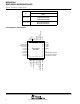
MSP430F23x0 MIXED SIGNAL MICROCONTROLLER SLAS518A -- AUGUST 2006 -- REVISED MAY 2007 AVAILABLE OPTIONS PACKAGED DEVICES TA PLASTIC 40-PIN QFN (RHA) --40°C to 85°C --40°C to 105°C MSP430F2330IRHA MSP430F2350IRHA MSP430F2370IRHA MSP430F2330TRHA MSP430F2350TRHA MSP430F2370TRHA AVCC D/AVSS RST/NMI TCK TMS TDI/TCLK TDO/TDI P4.7/TBCLK P4.6/TBOUTH/ACLK P4.5/TB2 pin designation, MSP430F23x0 P4.4/TB1 P4.3/TB0 P4.2/TB2 P1.0/TACLK P1.1/TA0 4 5 27 26 P4.1/TB1 P4.0/TB0 P1.2/TA1 P1.3/TA2 P1.
MSP430F23x0 MIXED SIGNAL MICROCONTROLLER SLAS518A -- AUGUST 2006 -- REVISED MAY 2007 functional block diagram MSP430F23x0 XIN XOUT DVCC D/AVSS AVCC P1.x/P2.x 2x8 P3.x/P4.x 2x8 ACLK Basic Clock System+ SMCLK Flash RAM 32kB 16kB 8kB 2kB 2kB 1kB MCLK 16MHz CPU MAB incl.
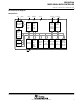
MSP430F23x0 MIXED SIGNAL MICROCONTROLLER SLAS518A -- AUGUST 2006 -- REVISED MAY 2007 Terminal Functions, MSP430F23x0 TERMINAL NAME NO DESCRIPTION I/O DVCC 1 XIN/P2.6/CA6 2 I/O Input terminal of crystal oscillator/general-purpose digital I/O pin/Comparator_A input XOUT/P2.7/CA7 3 I/O Output terminal of crystal oscillator/general-purpose digital I/O pin/Comparator_A input P1.0/TACLK 4 I/O General-purpose digital I/O pin/Timer_A, clock signal TACLK input P1.
MSP430F23x0 MIXED SIGNAL MICROCONTROLLER SLAS518A -- AUGUST 2006 -- REVISED MAY 2007 Terminal Functions (Continued) TERMINAL NAME DESCRIPTION NO I/O TCK 37 I Test clock. TCK is the clock input port for device programming and test.
MSP430F23x0 MIXED SIGNAL MICROCONTROLLER SLAS518A -- AUGUST 2006 -- REVISED MAY 2007 short-form description CPU The MSP430 CPU has a 16-bit RISC architecture that is highly transparent to the application. All operations, other than program-flow instructions, are performed as register operations in conjunction with seven addressing modes for source operand and four addressing modes for destination operand.
MSP430F23x0 MIXED SIGNAL MICROCONTROLLER SLAS518A -- AUGUST 2006 -- REVISED MAY 2007 operating modes The MSP430 has one active mode and five software selectable low-power modes of operation. An interrupt event can wake up the device from any of the five low-power modes, service the request and restore back to the low-power mode on return from the interrupt program.
MSP430F23x0 MIXED SIGNAL MICROCONTROLLER SLAS518A -- AUGUST 2006 -- REVISED MAY 2007 interrupt vector addresses The interrupt vectors and the power-up starting address are located in the address range 0xFFFF--0xFFC0. The vector contains the 16-bit address of the appropriate interrupt-handler instruction sequence.
MSP430F23x0 MIXED SIGNAL MICROCONTROLLER SLAS518A -- AUGUST 2006 -- REVISED MAY 2007 special function registers Most interrupt and module-enable bits are collected in the lowest address space. Special-function register bits not allocated to a functional purpose are not physically present in the device. This arrangement provides simple software access. interrupt enable 1 and 2 Address 7 6 00h 5 4 ACCVIE rw--0 3 2 1 0 NMIIE OFIE WDTIE rw--0 rw--0 rw--0 WDTIE Watchdog Timer interrupt enable.
MSP430F23x0 MIXED SIGNAL MICROCONTROLLER SLAS518A -- AUGUST 2006 -- REVISED MAY 2007 interrupt flag register 1 and 2 Address 7 6 5 02h 4 3 2 1 0 NMIIFG RSTIFG PORIFG OFIFG WDTIFG rw--0 rw--(0) rw--(1) rw--1 rw--(0) WDTIFG Set on Watchdog Timer overflow (in watchdog mode) or security key violation. Reset on VCC power-up or a reset condition at RST/NMI pin in reset mode. OFIFG Flag set on oscillator fault RSTIFG External reset interrupt flag.
MSP430F23x0 MIXED SIGNAL MICROCONTROLLER SLAS518A -- AUGUST 2006 -- REVISED MAY 2007 memory organization MSP430F2330 MSP430F2350 MSP430F2370 Memory Main: interrupt vector Main: code memory Size Flash Flash 8KB Flash 0xFFFF -- 0xFFC0 0xFFFF -- 0xE000 16KB Flash 0xFFFF -- 0xFFC0 0xFFFF -- 0xC000 32KB 0xFFFF -- 0xFFC0 0xFFFF -- 0x8000 Information memory Size Flash 256 Byte 0x10FF -- 0x1000 256 Byte 0x10FF -- 0x1000 256 Byte 0x10FF -- 0x1000 Boot memory Size ROM 1KB 0x0FFF -- 0x0C00 1KB 0x0FFF
MSP430F23x0 MIXED SIGNAL MICROCONTROLLER SLAS518A -- AUGUST 2006 -- REVISED MAY 2007 peripherals Peripherals are connected to the CPU through data, address, and control busses and can be handled using all instructions. For complete module descriptions, refer to the MSP430x2xx Family User’s Guide.
MSP430F23x0 MIXED SIGNAL MICROCONTROLLER SLAS518A -- AUGUST 2006 -- REVISED MAY 2007 hardware multiplier The multiplication operation is supported by a dedicated peripheral module. The module performs 16×16, 16×8, 8×16, and 8×8 bit operations. The module is capable of supporting signed and unsigned multiplication as well as signed and unsigned multiply and accumulate operations. The result of an operation can be accessed immediately after the operands have been loaded into the peripheral registers.
MSP430F23x0 MIXED SIGNAL MICROCONTROLLER SLAS518A -- AUGUST 2006 -- REVISED MAY 2007 timer_B3 Timer_B3 is a 16-bit timer/counter with three capture/compare registers. Timer_B3 can support multiple capture/compares, PWM outputs, and interval timing. Timer_B3 also has extensive interrupt capabilities. Interrupts may be generated from the counter on overflow conditions and from each of the capture/compare registers.
MSP430F23x0 MIXED SIGNAL MICROCONTROLLER SLAS518A -- AUGUST 2006 -- REVISED MAY 2007 peripheral file map PERIPHERALS WITH WORD ACCESS Timer_B3 Capture/compare register Capture/compare register Capture/compare register Timer_B register Capture/compare control Capture/compare control Capture/compare control Timer_B control Timer_B interrupt vector TBCCR2 TBCCR1 TBCCR0 TBR TBCCTL2 TBCCTL1 TBCCTL0 TBCTL TBIV 0x0196 0x0194 0x0192 0x0190 0x0186 0x0184 0x0182 0x0180 0x011E Timer_A3 Capture/compare register C
MSP430F23x0 MIXED SIGNAL MICROCONTROLLER SLAS518A -- AUGUST 2006 -- REVISED MAY 2007 PERIPHERALS WITH BYTE ACCESS (continued) 16 Basic Clock System+ Basic clock system control 3 Basic clock system control 2 Basic clock system control 1 DCO clock frequency control BCSCTL3 BCSCTL2 BCSCTL1 DCOCTL 0x0053 0x0058 0x0057 0x0056 Port P4 Port P4 resistor enable Port P4 selection Port P4 direction Port P4 output Port P4 input P4REN P4SEL P4DIR P4OUT P4IN 0x0011 0x001F 0x001E 0x001D 0x001C Port P3 Port P3
MSP430F23x0 MIXED SIGNAL MICROCONTROLLER SLAS518A -- AUGUST 2006 -- REVISED MAY 2007 absolute maximum ratings (see Note 1) Voltage applied at VCC to VSS . . . . . . . . . . . . . . . . . . . . . . . . . . . . . . . . . . . . . . . . . . . . . . . . . . . . --0.3 V to + 4.1 V Voltage applied to any pin (see Note 2) . . . . . . . . . . . . . . . . . . . . . . . . . . . . . . . . . . . . . . . . --0.3 V to VCC+0.3 V Diode current at any device terminal . . . . . . . . . . . . . . . . . . . . . . . . . . . . .
MSP430F23x0 MIXED SIGNAL MICROCONTROLLER SLAS518A -- AUGUST 2006 -- REVISED MAY 2007 electrical characteristics over recommended ranges of supply voltage and operating free-air temperature (unless otherwise noted) active mode supply current (into VCC) excluding external current (see Notes 1 and 2) PARAMETER IAM, 1MHz IAM, 1MHz IAM, 4kHz IAM,100kHz Active mode (AM) current (1MHz) Active mode (AM) current (1MHz) Active mode (AM) current (4kHz) Active mode (AM) current (100kHz) TEST CONDITIONS TA f
MSP430F23x0 MIXED SIGNAL MICROCONTROLLER SLAS518A -- AUGUST 2006 -- REVISED MAY 2007 typical characteristics -- active mode supply current (into DVCC + AVCC) 8.0 5.0 fDCO = 16 MHz 6.0 fDCO = 12 MHz 5.0 4.0 fDCO = 8 MHz 3.0 2.0 0.0 1.5 2.0 2.5 3.0 3.5 4.0 TA = 25 °C 3.0 VCC = 3 V 2.0 TA = 85 °C TA = 25 °C 1.0 fDCO = 1 MHz 1.0 TA = 85 °C Active Mode Current -- mA Active Mode Current -- mA 7.0 VCC = 2.2 V 4.0 0.0 0.0 VCC -- Supply Voltage -- V Figure 2.
MSP430F23x0 MIXED SIGNAL MICROCONTROLLER SLAS518A -- AUGUST 2006 -- REVISED MAY 2007 electrical characteristics over recommended ranges of supply voltage and operating free-air temperature (unless otherwise noted) low power mode supply currents (into VCC) excluding external current (see Notes 1 and 2) PARAMETER ILPM0, 1MHz ILPM0, 100kHz ILPM2 Low-power mode 0 (LPM0) current, current see Note 3 Low-power mode 0 (LPM0) current, current see Note 3 Low-power mode 2 (LPM2) current, current see Note 4 TES
MSP430F23x0 MIXED SIGNAL MICROCONTROLLER SLAS518A -- AUGUST 2006 -- REVISED MAY 2007 electrical characteristics over recommended ranges of supply voltage and operating free-air temperature (unless otherwise noted) Schmitt-trigger inputs -- Ports P1, P2, P3 P4, JTAG, RST/NMI, and XIN (see Note) PARAMETER VIT+ VIT-- TEST CONDITIONS Positive-going P iti i input i t threshold th h ld voltage Negative-going N ti i input i t threshold th h ld voltage Vhys Input voltage hysteresis (VIT+ -- VIT-- ) RPull P
MSP430F23x0 MIXED SIGNAL MICROCONTROLLER SLAS518A -- AUGUST 2006 -- REVISED MAY 2007 electrical characteristics over recommended ranges of supply voltage and operating free-air temperature (unless otherwise noted) (continued) outputs -- Ports P1, P2, P3 and P4 PARAMETER VOH VOL High level output High-level voltage Low level output Low-level voltage VCC MIN I(OHmax) = --1.5 mA (see Notes 1) TEST CONDITIONS 2.2 V VCC --0.25 TYP MAX VCC UNIT I(OHmax) = --6 mA (see Notes 2) 2.2 V VCC --0.
MSP430F23x0 MIXED SIGNAL MICROCONTROLLER SLAS518A -- AUGUST 2006 -- REVISED MAY 2007 electrical characteristics over recommended ranges of supply voltage and operating free-air temperature (unless otherwise noted) (continued) typical characteristics -- outputs TYPICAL LOW-LEVEL OUTPUT CURRENT vs LOW-LEVEL OUTPUT VOLTAGE TYPICAL LOW-LEVEL OUTPUT CURRENT vs LOW-LEVEL OUTPUT VOLTAGE 50.0 TA = 25°C VCC = 2.2 V P2.4 20.
MSP430F23x0 MIXED SIGNAL MICROCONTROLLER SLAS518A -- AUGUST 2006 -- REVISED MAY 2007 electrical characteristics over recommended ranges of supply voltage and operating free-air temperature (unless otherwise noted) (continued) POR/brownout reset (BOR) (see Notes 1 and 2) PARAMETER TEST CONDITIONS VCC(start) (see Figure 8) dVCC/dt ≤ 3 V/s V(B_IT--) (see Figure 8 through Figure 10) dVCC/dt ≤ 3 V/s Vhys(B_IT--) (see Figure 8) dVCC/dt ≤ 3 V/s td(BOR) (see Figure 8) t(reset) Pulse length needed at
MSP430F23x0 MIXED SIGNAL MICROCONTROLLER SLAS518A -- AUGUST 2006 -- REVISED MAY 2007 electrical characteristics over recommended ranges of supply voltage and operating free-air temperature (unless otherwise noted) (continued) typical characteristics -- POR/brownout reset (BOR) VCC 3V VCC(drop) -- V 2 VCC = 3 V Typical Conditions 1.5 t pw 1 VCC(drop) 0.5 0 0.001 1 1000 1 ns tpw -- Pulse Width -- μs 1 ns tpw -- Pulse Width -- μs Figure 9.
MSP430F23x0 MIXED SIGNAL MICROCONTROLLER SLAS518A -- AUGUST 2006 -- REVISED MAY 2007 electrical characteristics over recommended ranges of supply voltage and operating free-air temperature (unless otherwise noted) (continued) main DCO characteristics D All ranges selected by RSELx overlap with RSELx + 1: RSELx = 0 overlaps RSELx = 1, ... RSELx = 14 overlaps RSELx = 15. D DCO control bits DCOx have a step size as defined by parameter SDCO.
MSP430F23x0 MIXED SIGNAL MICROCONTROLLER SLAS518A -- AUGUST 2006 -- REVISED MAY 2007 electrical characteristics over recommended ranges of supply voltage and operating free-air temperature (unless otherwise noted) (continued) calibrated DCO frequencies -- tolerance at calibration PARAMETER TEST CONDITIONS Frequency tolerance at calibration TA VCC MIN TYP MAX UNIT 25°C 3V --1 ±0.2 +1 % 25°C 3V 0.990 1 1.
MSP430F23x0 MIXED SIGNAL MICROCONTROLLER SLAS518A -- AUGUST 2006 -- REVISED MAY 2007 electrical characteristics over recommended ranges of supply voltage and operating free-air temperature (unless otherwise noted) (continued) calibrated DCO frequencies -- tolerance over supply voltage VCC PARAMETER TEST CONDITIONS TA VCC MIN TYP MAX UNIT 1 MHz tolerance over VCC 25°C 1.8 V -- 3.6 V --3 ±2 +3 % 8 MHz tolerance over VCC 25°C 1.8 V -- 3.6 V --3 ±2 +3 % 12 MHz tolerance over VCC 25°C 2.
MSP430F23x0 MIXED SIGNAL MICROCONTROLLER SLAS518A -- AUGUST 2006 -- REVISED MAY 2007 1.03 Frequency -- MHz 1.02 TA = 105 °C 1.01 TA = 85 °C 1.00 TA = 25 °C 0.99 TA = --40 °C 0.98 0.97 1.5 2.0 2.5 3.0 3.5 4.0 VCC -- Supply Voltage -- V Figure 11. Calibrated 1 MHz Frequency vs.
MSP430F23x0 MIXED SIGNAL MICROCONTROLLER SLAS518A -- AUGUST 2006 -- REVISED MAY 2007 ,electrical characteristics over recommended ranges of supply voltage and operating free-air temperature (unless otherwise noted) (continued) wake-up from lower power modes (LPM3/4) PARAMETER tDCO,LPM3/4 tCPU,LPM3/4 TEST CONDITIONS DCO clock wake--up time from LPM3/4 (see Note 1) VCC MIN TYP MAX BCSCTL1= CALBC1_1MHZ; DCOCTL = CALDCO_1MHZ 2.2 V/3 V 2 BCSCTL1= CALBC1_8MHZ; DCOCTL = CALDCO_8MHZ 2.2 V/3 V 1.
MSP430F23x0 MIXED SIGNAL MICROCONTROLLER SLAS518A -- AUGUST 2006 -- REVISED MAY 2007 electrical characteristics over recommended ranges of supply voltage and operating free-air temperature (unless otherwise noted) (continued) DCO with external resistor ROSC (see Note) PARAMETER TEST CONDITIONS VCC fDCO,ROSC DCO output frequency with ROSC DCOR = 1, RSELx = 4, 4 DCOx = 3, 3 MODx = 0 0, TA = 25°C Dt Temperature drift DV Drift with VCC MIN TYP MAX UNIT 2.2 V 1.8 3V 1.
MSP430F23x0 MIXED SIGNAL MICROCONTROLLER SLAS518A -- AUGUST 2006 -- REVISED MAY 2007 electrical characteristics over recommended ranges of supply voltage and operating free-air temperature (unless otherwise noted) (continued) crystal oscillator, LFXT1, low frequency modes (see Note 4) PARAMETER TEST CONDITIONS VCC fLFXT1,LF LFXT1 oscillator crystal frequency, LF mode 0, 1 XTS = 0, LFXT1Sx = 0 or 1 1.8 V -- 3.
MSP430F23x0 MIXED SIGNAL MICROCONTROLLER SLAS518A -- AUGUST 2006 -- REVISED MAY 2007 electrical characteristics over recommended ranges of supply voltage and operating free-air temperature (unless otherwise noted) (continued) crystal oscillator, LFXT1, high frequency modes (see Note 5) PARAMETER TEST CONDITIONS VCC MIN TYP MAX UNIT fLFXT1,HF0 LFXT1 oscillator crystal frequency, HF mode 0 XTS = 1, XCAPx = 0, LFXT1Sx = 0 1.8 V -- 3.6 V 0.
MSP430F23x0 MIXED SIGNAL MICROCONTROLLER SLAS518A -- AUGUST 2006 -- REVISED MAY 2007 electrical characteristics over recommended ranges of supply voltage and operating free-air temperature (unless otherwise noted) (continued) typical characteristics -- LFXT1 oscillator in HF mode (XTS = 1) Oscillation Allowance -- Ohms 100000.00 10000.00 1000.00 LFXT1Sx = 3 100.00 LFXT1Sx = 2 LFXT1Sx = 1 10.00 0.10 1.00 10.00 100.00 Crystal Frequency -- MHz Figure 17.
MSP430F23x0 MIXED SIGNAL MICROCONTROLLER SLAS518A -- AUGUST 2006 -- REVISED MAY 2007 electrical characteristics over recommended ranges of supply voltage and operating free-air temperature (unless otherwise noted) (continued) Timer_A PARAMETER TEST CONDITIONS fTA Timer A clock frequency Timer_A Internal: SMCLK, ACLK; External: TACLK, TACLK INCLK; Duty Cycle = 50% ±10% tTA,cap Timer_A, capture timing TA0, TA1, TA2 VCC MIN TYP MAX 2.2 V 10 3V 16 2.
MSP430F23x0 MIXED SIGNAL MICROCONTROLLER SLAS518A -- AUGUST 2006 -- REVISED MAY 2007 electrical characteristics over recommended ranges of supply voltage and operating free-air temperature (unless otherwise noted) (continued) USCI (UART Mode) PARAMETER fUSCI USCI input clock frequency fBITCLK BITCLK clock frequency (equals baudrate in MBaud) tτ UART receive deglitch time (see Note NO TAG) TEST CONDITIONS VCC MIN TYP Internal: SMCLK, ACLK External: UCLK Duty Cycle = 50% ± 10% 2.
MSP430F23x0 MIXED SIGNAL MICROCONTROLLER SLAS518A -- AUGUST 2006 -- REVISED MAY 2007 electrical characteristics over recommended ranges of supply voltage and operating free-air temperature (unless otherwise noted) (continued)6 1/fUCxCLK CKPL =0 CKPL =1 UCLK tLOW/HIGH tLOW/HIGH tSU,MI tHD,MI SOMI tVALID ,MO SIMO Figure 19. SPI Master Mode, CKPH = 0 1/fUCxCLK CKPL =0 CKPL =1 UCLK tLOW/HIGH tLOW/HIGH tSU,MI tHD,MI SOMI tVALID ,MO SIMO Figure 20.
MSP430F23x0 MIXED SIGNAL MICROCONTROLLER SLAS518A -- AUGUST 2006 -- REVISED MAY 2007 electrical characteristics over recommended ranges of supply voltage and operating free-air temperature (unless otherwise noted) (continued)7 tSTE,LEAD tSTE,LAG STE 1/fUCxCLK CKPL =0 CKPL =1 UCLK tLOW/HIGH tLOW/HIGH tSU,SIMO tHD,SIMO SIMO tACC tVALID ,SOMI tDIS SOMI Figure 21.
MSP430F23x0 MIXED SIGNAL MICROCONTROLLER SLAS518A -- AUGUST 2006 -- REVISED MAY 2007 electrical characteristics over recommended ranges of supply voltage and operating free-air temperature (unless otherwise noted) (continued) USCI (I2C Mode, see Figure 23) PARAMETER TEST CONDITIONS fUSCI USCI input clock frequency fSCL SCL clock frequency VCC MIN TYP Internal: SMCLK, ACLK External: UCLK Duty Cycle = 50% ± 10% MAX UNIT fSYSTEM MHz 400 kHz 2.2 V/3 V 0 fSCL ≤ 100kHz 2.2 V/3 V 4.
MSP430F23x0 MIXED SIGNAL MICROCONTROLLER SLAS518A -- AUGUST 2006 -- REVISED MAY 2007 electrical characteristics over recommended ranges of supply voltage and operating free-air temperature (unless otherwise noted) (continued) Comparator_A+ (see Note 1) PARAMETER TEST CONDITIONS I(DD) CAON 1 CARSEL=0, CAON=1, CARSEL 0 CAREF=0 CAREF 0 I(Refladder/RefDiode) CAON=1, CARSEL=0, CAREF 1/2/3 CAREF=1/2/3, no load at P1.0/CA0 and P1.1/CA1 V(IC) V(Ref025) V(Ref050) VCC MIN TYP MAX 2.
MSP430F23x0 MIXED SIGNAL MICROCONTROLLER SLAS518A -- AUGUST 2006 -- REVISED MAY 2007 electrical characteristics over recommended ranges of supply voltage and operating free-air temperature (unless otherwise noted) (continued) 0V VCC 0 1 CAF CAON To Internal Modules Low Pass Filter + _ V+ V-- 0 0 1 1 CAOUT Set CAIFG Flag τ ≈ 2.0 μs Figure 24. Block Diagram of Comparator_A+ Module VCAOUT Overdrive V-400 mV t(response) V+ Figure 25.
MSP430F23x0 MIXED SIGNAL MICROCONTROLLER SLAS518A -- AUGUST 2006 -- REVISED MAY 2007 electrical characteristics over recommended ranges of supply voltage and operating free-air temperature (unless otherwise noted) (continued) typical characteristics -- Comparator_A+ 650 650 VCC = 2.
MSP430F23x0 MIXED SIGNAL MICROCONTROLLER SLAS518A -- AUGUST 2006 -- REVISED MAY 2007 electrical characteristics over recommended ranges of supply voltage and operating free-air temperature (unless otherwise noted) (continued) Flash Memory PARAMETER VCC(PGM/ TEST CONDITIONS VCC Program and erase supply voltage ERASE) MIN TYP 2.2 fFTG Flash Timing Generator frequency IPGM Supply current from VCC during program 2.2 V/3.6 V 257 1 IERASE Supply current from VCC during erase 2.2 V/3.
MSP430F23x0 MIXED SIGNAL MICROCONTROLLER SLAS518A -- AUGUST 2006 -- REVISED MAY 2007 APPLICATION INFORMATION Port P1 pin schematic: P1.0 to P1.7, input/output with Schmitt-trigger Pad Logic P1REN.x P1DIR.x 0 0 Module X OUT 1 0 DVCC 1 P1.0/TACLK P1.1/TA0 P1.2/TA1 P1.3/TA2 P1.4/SMCLK P1.5/TA0 P1.6/TA1 P1.7/TA2 P1SEL.x P1IN.x EN Module X IN D P1IE.x P1IRQ.x EN Q P1IFG.x P1SEL.x P1IES.x 44 1 Direction 0: Input 1: Output 1 P1OUT.
MSP430F23x0 MIXED SIGNAL MICROCONTROLLER SLAS518A -- AUGUST 2006 -- REVISED MAY 2007 Port P1 (P1.0 to P1.7) pin functions PIN NAME (P1.X) (P1 X) P1.0/TACLK / X 0 FUNCTION P1.0 (I/O) Timer_A3.TACLK DVSS P1.1/TA0 / P1.2/TA1 / P1.3/TA2 / 1 2 3 P1.4/SMCLK / 4 P1.5/TA0 / 5 P1.7/TA2 / 6 7 P1DIR.x P1SEL.x I: 0; O: 1 0 0 1 1 1 I: 0; O: 1 0 Timer_A3.CCI0A 0 1 Timer_A3.TA0 1 1 I: 0; O: 1 0 Timer_A3.CCI0A 0 1 Timer_A3.TA0 1 1 I: 0; O: 1 0 Timer_A3.CCI0A 0 1 Timer_A3.
MSP430F23x0 MIXED SIGNAL MICROCONTROLLER SLAS518A -- AUGUST 2006 -- REVISED MAY 2007 Port P2 pin schematic: P2.0 -- P2.4, input/output with Schmitt-trigger Pad Logic To Comparator_A From Comparator_A CAPD.x P2REN.x P2DIR.x 0 0 Module X OUT 1 0 DVCC 1 Bus Keeper EN P2SEL.x P2IN.x EN Module X IN D P2IE.x P2IRQ.x EN Q P2IFG.x P2SEL.x P2IES.x 46 1 Direction 0: Input 1: Output 1 P2OUT.x DVSS Set Interrupt Edge Select POST OFFICE BOX 655303 • DALLAS, TEXAS 75265 P2.0/ACLK/CA2 P2.
MSP430F23x0 MIXED SIGNAL MICROCONTROLLER SLAS518A -- AUGUST 2006 -- REVISED MAY 2007 Port P2.0 -- P2.4 pin functions PIN NAME (P2.X) (P2 X) P2.0/ACLK/CA2 / / P2.1/TAINCLK/CA3 / / P2.2/CAOUT/TA0/ / / / CA4 P2.3/CA0/TA1 / / P2.4/CA1/TA2 / / X 0 1 2 3 4 CONTROL BITS / SIGNALS FUNCTION CAPD.x P2DIR.x P2SEL.x P2.0 (I/O) 0 I: 0; O: 1 0 ACLK 0 1 1 CA2 (see Note 2) 1 X X P2.1 (I/O) 0 I: 0; O: 1 0 Timer_A3.TAINCLK 0 0 1 DVSS 0 1 1 CA3 (see Note 2) 1 X X P2.
MSP430F23x0 MIXED SIGNAL MICROCONTROLLER SLAS518A -- AUGUST 2006 -- REVISED MAY 2007 Port P2 pin schematic: P2.5, input/output with Schmitt-trigger Pad Logic To Comparator From Comparator CAPD.5 To DCO DCOR in DCO P2REN.5 P2DIR.5 0 0 Module X OUT 1 0 DVCC 1 1 Direction 0: Input 1: Output 1 P2OUT.5 DVSS P2.5/ROSC/CA5 Bus Keeper EN P2SEL.x P2IN.5 EN Module X IN D P2IE.5 P2IRQ.5 EN Q Set P2IFG.5 P2SEL.5 Interrupt Edge Select P2IES.5 Port P2.5 pin functions PIN NAME (P2.X) (P2 X) P2.
MSP430F23x0 MIXED SIGNAL MICROCONTROLLER SLAS518A -- AUGUST 2006 -- REVISED MAY 2007 Port P2 pin schematic: P2.6, input/output with Schmitt-trigger BCSCTL3.LFXT1Sx = 11 P2.7/XOUT/CA7 LFXT1 off 0 LFXT1CLK 1 Pad Logic To Comparator From Comparator CAPD.6 P2SEL.7 P2REN.6 P2DIR.6 0 0 Module X OUT 1 0 DVCC 1 1 Direction 0: Input 1: Output 1 P2OUT.6 DVSS P2.6/XIN/CA6 Bus Keeper EN P2SEL.6 P2IN.6 EN Module X IN D P2IE.6 P2IRQ.6 EN Q P2IFG.6 P2SEL.6 P2IES.
MSP430F23x0 MIXED SIGNAL MICROCONTROLLER SLAS518A -- AUGUST 2006 -- REVISED MAY 2007 Port P2.6 pin functions PIN NAME (P2.X) (P2 X) P2.6/XIN/CA6 / / X 6 CONTROL BITS / SIGNALS FUNCTION CAPD.6 P2DIR.6 P2SEL.6 P2.6 (I/O) 0 I: 0; O: 1 0 XIN (default) X 1 1 CA6 (see Note 2) 1 X 0 NOTES: 1. X: Don’t care. 2. Setting the CAPD.x bit disables the output driver as well as the input to prevent parasitic cross currents when applying analog signals.
MSP430F23x0 MIXED SIGNAL MICROCONTROLLER SLAS518A -- AUGUST 2006 -- REVISED MAY 2007 Port P2 pin schematic: P2.7, input/output with Schmitt-trigger BCSCTL3.LFXT1Sx = 11 P2.6/XIN/TA1 LFXT1 off 0 LFXT1CLK From P2.6/XIN 1 Pad Logic To Comparator From Comparator CAPD.7 P2SEL.6 P2REN.7 P2DIR.7 0 0 Module X OUT 1 0 DVCC 1 1 Direction 0: Input 1: Output 1 P2OUT.7 DVSS P2.7/XOUT Bus Keeper EN P2SEL.7 P2IN.7 EN Module X IN D P2IE.7 P2IRQ.7 EN Q P2IFG.7 P2SEL.7 P2IES.
MSP430F23x0 MIXED SIGNAL MICROCONTROLLER SLAS518A -- AUGUST 2006 -- REVISED MAY 2007 Port P2.7 pin functions PIN NAME (P2.X) (P2 X) P2.7/XOUT/CA7 / / X 7 CONTROL BITS / SIGNALS FUNCTION CAPD.7 P2DIR.7 P2SEL.7 P2.7 (I/O) 0 I: 0; O: 1 0 XOUT (default) X 1 1 CA7 (see Note 2) 1 X 0 NOTES: 1. X: Don’t care. 2. Setting the CAPD.x bit disables the output driver as well as the input to prevent parasitic cross currents when applying analog signals.
MSP430F23x0 MIXED SIGNAL MICROCONTROLLER SLAS518A -- AUGUST 2006 -- REVISED MAY 2007 Port P3 pin schematic: P3.0 to P3.5, input/output with Schmitt-trigger Pad Logic P3REN.x P3DIR.x 0 Module direction 1 P3OUT.x 0 Module X OUT DVSS 0 DVCC 1 1 Direction 0: Input 1: Output 1 P3.0/UCB0STE/UCA0CLK P3.1/UCB0SIMO/UCB0SDA P3.2/UCB0SOMI/UCB0SCL P3.3/UCB0CLK/UCA0STE P3.4/UCA0TXD/UCA0SIMO P3.5/UCA0RXD/UCA0SOMI P3SEL.x P3IN.x EN Module X IN D Port P3.0 to P3.5 pin functions PIN NAME (P3.
MSP430F23x0 MIXED SIGNAL MICROCONTROLLER SLAS518A -- AUGUST 2006 -- REVISED MAY 2007 Port P3 pin schematic: P3.6 to P3.7, input/output with Schmitt-trigger Pad Logic P3REN.x P3DIR.x 0 0 1 P3OUT.x 0 Module X OUT DVSS 0 DVCC 1 1 Direction 0: Input 1: Output 1 P3.6 P3.7 P3SEL.x P3IN.x EN Module X IN D Port P3.6 to P3.7 pin functions PIN NAME (P3.X) X FUNCTION P3DIR.x P3SEL.x P3.6 6 P3.6 (I/O) I: 0; O: 1 0 P3.7 7 P3.
MSP430F23x0 MIXED SIGNAL MICROCONTROLLER SLAS518A -- AUGUST 2006 -- REVISED MAY 2007 Port P4 pin schematic: P4.0 to P4.7, input/output with Schmitt-trigger Pad Logic P4REN.x P4DIR.x 0 0 Module X OUT 1 0 DVCC 1 1 Direction 0: Input 1: Output 1 P4OUT.x DVSS P4.0/TB0 P4.1/TB1 P4.2/TB2 P4.3/TB0 P4.4/TB1 P4.5/TB2 P4.6/TBOUTH/ACLK P4.7/TBCLK/ TBINCLK P4SEL.x P4IN.x EN Module X IN D Port P4.0 to P4.7 pin functions PIN NAME (P4.X) (P4 X) P4.0/TB0 / P4.1/TB1 / P4.2/TB2 / P4.3/TB0 / P4.
MSP430F23x0 MIXED SIGNAL MICROCONTROLLER SLAS518A -- AUGUST 2006 -- REVISED MAY 2007 APPLICATION INFORMATION JTAG pins TMS, TCK, TDI/TCLK, TDO/TDI, input/output with Schmitt-trigger TDO Controlled by JTAG Controlled by JTAG JTAG TDO/TDI Controlled by JTAG DVCC DVCC TDI Fuse Burn & Test Fuse Test TDI/TCLK & Emulation Module DVCC TMS TMS DVCC During Programming Activity and During Blowing of the Fuse, Pin TDO/TDI Is Used to Apply the Test Input Data for JTAG Circuitry TCK TCK 56 POST OFFICE BOX 6
MSP430F23x0 MIXED SIGNAL MICROCONTROLLER SLAS518A -- AUGUST 2006 -- REVISED MAY 2007 APPLICATION INFORMATION JTAG fuse check mode MSP430F23x0 devices that have the fuse on the TDI/TCLK terminal have a fuse check mode that tests the continuity of the fuse the first time the JTAG port is accessed after a power-on reset (POR). When activated, a fuse check current, ITF, of 1 mA at 3 V, 2.5 mA at 5 V can flow from the TDI/TCLK pin to ground if the fuse is not burned.
MSP430F23x0 MIXED SIGNAL MICROCONTROLLER SLAS518A -- AUGUST 2006 -- REVISED MAY 2007 Data Sheet Revision History LITERATURE NUMBER SUMMARY SLAS518 Preliminary PRODUCT PREVIEW data sheet release. SLAS518A PRODUCTION DATA data sheet release.
PACKAGE OPTION ADDENDUM www.ti.
PACKAGE OPTION ADDENDUM www.ti.com 18-May-2007 In no event shall TI's liability arising out of such information exceed the total purchase price of the TI part(s) at issue in this document sold by TI to Customer on an annual basis.
IMPORTANT NOTICE Texas Instruments Incorporated and its subsidiaries (TI) reserve the right to make corrections, modifications, enhancements, improvements, and other changes to its products and services at any time and to discontinue any product or service without notice. Customers should obtain the latest relevant information before placing orders and should verify that such information is current and complete.