MSP430F41x2 MIXED SIGNAL MICROCONTROLLER SLAS648E -- APRIL 2009 -- REVISED MARCH 2011 D Low Supply-Voltage Range, 1.8 V to 3.6 V D Ultralow Power Consumption D D D D D D D Active Mode: 220 A at 1 MHz, 2.2 V Standby Mode: 0.9 A Off Mode (RAM Retention): 0.
MSP430F41x2 MIXED SIGNAL MICROCONTROLLER SLAS648E -- APRIL 2009 -- REVISED MARCH 2011 AVAILABLE OPTIONS† PACKAGED DEVICES‡ TA --40C to 85C PLASTIC 64-PIN QFP (PM) PLASTIC 48-PIN QFN (RGZ) MSP430F4152IPM MSP430F4132IPM MSP430F4152IRGZ MSP430F4132IRGZ † For the most current package and ordering information, see the Package Option Addendum at the end of this document, or see the TI web site at www.ti.com. ‡ Package drawings, thermal data, and symbolization are available at www.ti.com/packaging.
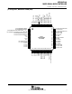
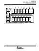
MSP430F41x2 MIXED SIGNAL MICROCONTROLLER SLAS648E -- APRIL 2009 -- REVISED MARCH 2011 AVCC P6.0/TA1.2/A2/CA4 AVSS P7.5/TA1.3/A1/CA3 P7.4/TA1.4/A0/CA2 TEST/SBWTCLK RST/NMI/SBWTDIO P7.3/TCK/S35 P7.2/TMS/S34 P7.1/TDI/TCLK/S33 P7.0/TDO/TDI/S32 P1.0/TA0.0/S31 P1.1/TA0.0/MCLK/S30 P1.2/TA0.1/S29 P1.3/TA1.0/SVSOUT/S28 P1.4/TA1.
MSP430F41x2 MIXED SIGNAL MICROCONTROLLER SLAS648E -- APRIL 2009 -- REVISED MARCH 2011 P7.0/TDO/TDI/S32 P1.0/TA0.0/S31 P7.1/TDI/TCLK/S33 P7.2/TMS/S34 P7.3/TCK/S35 TEST/SBWTCLK RST/NMI/SBWTDIO P7.4/TA1.4/A0/CA2 AVSS P7.5/TA1.3/A1/CA3 P6.0/TA1.2/A2/CA4 AVCC pin designation, MSP430F41x2IRGZ (QFN)† 48 47 46 45 44 43 42 41 40 39 38 37 P6.1 1 36 P1.1/TA0.0/MCLK/S30 P6.2 2 35 P1.5/TA0CLK/CAOUT/S26 DVCC 3 34 P1.6/ACLK/CA0 XIN 4 33 P1.
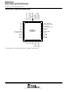
MSP430F41x2 MIXED SIGNAL MICROCONTROLLER SLAS648E -- APRIL 2009 -- REVISED MARCH 2011 functional block diagram XIN XOUT DVCC DVSS AVCC AVSS P1.x/P2.x 2x8 P3.x/P4.x 2x8 P5.x/P6.x P7.x 1x7 2x8 ACLK Oscillators FLL+ VLO ADC10 SMCLK Flash RAM 16kB 8kB 512B 512B Brownout Protection LCD_A 144 Segments 1,2,3,4 Mux MCLK CPU 64kB MAB incl.
MSP430F41x2 MIXED SIGNAL MICROCONTROLLER SLAS648E -- APRIL 2009 -- REVISED MARCH 2011 Terminal Functions TERMINAL NO. I/O DESCRIPTION 37 I/O General-purpose digital I/O pin Timer0_A3, capture: CCI0A input, compare: Out0 output LCD segment output 52 36 I/O General-purpose digital I/O pin Timer0_A3, capture: CCI0B input MCLK signal output LCD segment output P1.2/TA0.1/S29 51 -- I/O General-purpose digital I/O pin Timer0_A3, capture: CCI1A input, compare: Out1 output LCD segment output P1.
MSP430F41x2 MIXED SIGNAL MICROCONTROLLER SLAS648E -- APRIL 2009 -- REVISED MARCH 2011 Terminal Functions (continued) TERMINAL NO.
MSP430F41x2 MIXED SIGNAL MICROCONTROLLER SLAS648E -- APRIL 2009 -- REVISED MARCH 2011 Terminal Functions (continued) TERMINAL NO. NAME I/O DESCRIPTION 64 PIN 48 PIN P5.3/R03 40 29 I/O General-purpose digital I/O pin input port of the fourth most positive analog LCD level (V1) P5.4/COM3 39 28 I/O General-purpose digital I/O pin common output, COM0--3 are used for LCD backplanes P5.5/COM2 38 27 I/O General-purpose digital I/O pin common output, COM0--3 are used for LCD backplanes P5.
MSP430F41x2 MIXED SIGNAL MICROCONTROLLER SLAS648E -- APRIL 2009 -- REVISED MARCH 2011 Terminal Functions (continued) TERMINAL NO. NAME I/O DESCRIPTION 64 PIN 48 PIN P7.3/TCK/S35 57 41 I/O P7.4/TA1.4/ A0/CA2 60 44 I/O General-purpose digital I/O pin Timer1_A5, capture: CCI4B input, compare: Out4 output ADC10 analog input A0 Comparator_A input 2 General-purpose digital I/O pin Test clock input for device programming and test LCD segment output P7.5/TA1.
MSP430F41x2 MIXED SIGNAL MICROCONTROLLER SLAS648E -- APRIL 2009 -- REVISED MARCH 2011 short-form description CPU The MSP430 CPU has a 16-bit RISC architecture that is highly transparent to the application. All operations, other than program-flow instructions, are performed as register operations in conjunction with seven addressing modes for source operand and four addressing modes for destination operand.
MSP430F41x2 MIXED SIGNAL MICROCONTROLLER SLAS648E -- APRIL 2009 -- REVISED MARCH 2011 operating modes The MSP430 has one active mode and five software selectable low-power modes of operation. An interrupt event can wake up the device from any of the five low-power modes, service the request, and restore back to the low-power mode on return from the interrupt program.
MSP430F41x2 MIXED SIGNAL MICROCONTROLLER SLAS648E -- APRIL 2009 -- REVISED MARCH 2011 interrupt vector addresses The interrupt vectors and the power-up starting address are located in the address range 0xFFFF to 0xFFC0. The vector contains the 16-bit address of the appropriate interrupt-handler instruction sequence. If the reset vector (located at address 0xFFFE) contains 0xFFFF (e.g., flash is not programmed), the CPU goes into LPM4 immediately after power-up.
MSP430F41x2 MIXED SIGNAL MICROCONTROLLER SLAS648E -- APRIL 2009 -- REVISED MARCH 2011 special function registers Most interrupt and module-enable bits are collected in the lowest address space. Special-function register bits not allocated to a functional purpose are not physically present in the device. This arrangement provides simple software access.
MSP430F41x2 MIXED SIGNAL MICROCONTROLLER SLAS648E -- APRIL 2009 -- REVISED MARCH 2011 interrupt flag register 1 and 2 Address 7 6 5 02h 4 3 2 1 0 NMIIFG RSTIFG PORIFG OFIFG WDTIFG rw--0 rw--(0) rw--(1) rw--1 rw--(0) WDTIFG Set on watchdog timer overflow (in watchdog mode) or security key violation. Reset on VCC power-up or a reset condition at RST/NMI pin in reset mode. OFIFG Flag set on oscillator fault RSTIFG External reset interrupt flag.
MSP430F41x2 MIXED SIGNAL MICROCONTROLLER SLAS648E -- APRIL 2009 -- REVISED MARCH 2011 memory organization MSP430F4152 MSP430F4132 Memory Main: interrupt vector Main: code memory Size Flash Flash 16KB 0FFFFh -- 0FFE0h 0FFFFh -- 0C000h 8KB 0FFFFh -- 0FFE0h 0FFFFh -- 0E000h Information memory Size Flash 256 Byte 010FFh -- 01000h 256 Byte 010FFh -- 01000h Boot memory Size ROM 1KB 0FFFh -- 0C00h 1KB 0FFFh -- 0C00h Size 512B 03FFh -- 0200h 512B 03FFh -- 0200h 16-bit 8-bit 8-bit SFR 01FFh -- 010
MSP430F41x2 MIXED SIGNAL MICROCONTROLLER SLAS648E -- APRIL 2009 -- REVISED MARCH 2011 peripherals Peripherals are connected to the CPU through data, address, and control buses and can be handled using all instructions. For complete module descriptions, see the MSP430x4xx Family User’s Guide, literature number SLAU056.
MSP430F41x2 MIXED SIGNAL MICROCONTROLLER SLAS648E -- APRIL 2009 -- REVISED MARCH 2011 watchdog timer (WDT+) The primary function of the WDT+ module is to perform a controlled system restart after a software problem occurs. If the selected time interval expires, a system reset is generated. If the watchdog function is not needed in an application, the module can be configured as an interval timer and can generate interrupts at selected time intervals.
MSP430F41x2 MIXED SIGNAL MICROCONTROLLER SLAS648E -- APRIL 2009 -- REVISED MARCH 2011 Timer1_A5 Timer_A5 is a 16-bit timer/counter with five capture/compare registers. Timer_A5 can support multiple capture/compares, PWM outputs, and interval timing. Timer_A5 also has extensive interrupt capabilities. Interrupts may be generated from the counter on overflow conditions and from each of the capture/compare registers. TIMER_A5 SIGNAL CONNECTIONS INPUT PIN NUMBER PM RGZ DEVICE INPUT SIGNAL 32 -- P3.
MSP430F41x2 MIXED SIGNAL MICROCONTROLLER SLAS648E -- APRIL 2009 -- REVISED MARCH 2011 ADC10 The ADC10 module supports fast 10-bit analog-to-digital conversions. The module implements a 10-bit SAR core, sample select control, reference generator, and data transfer controller (DTC) for automatic conversion result handling, allowing ADC samples to be converted and stored without any CPU intervention.
MSP430F41x2 MIXED SIGNAL MICROCONTROLLER SLAS648E -- APRIL 2009 -- REVISED MARCH 2011 peripheral file map (continued) PERIPHERALS WITH BYTE ACCESS LCD_A USCI A0/B0 / Comparator_A+ p _ 20 LCD Voltage Control 1 LCD Voltage Control 0 LCD Voltage Port Control 1 LCDAVCTL1 LCDAVCTL0 LCDAPCTL1 0AFh 0AEh 0ADh LCD Voltage Port Control 0 LCD memory 20 : LCD memory 16 LCDAPCTL0 LCDM20 : LCDM16 0ACh 0A4h : 0A0h LCD memory 15 : LCD memory 1 LCD control and mode LCDM15 : LCDM1 LCDACTL 09Fh : 091h 090h USCI
MSP430F41x2 MIXED SIGNAL MICROCONTROLLER SLAS648E -- APRIL 2009 -- REVISED MARCH 2011 peripheral file map (continued) PERIPHERALS WITH BYTE ACCESS RTC (Basic Timer1) Port P7 Port P6 Port P5 Port P4 Port P3 Port P2 Real Time Clock Year High Byte Real Time Clock Year Low Byte Real Time Clock Month RTCYEARH RTCYEARL RTCMON 04Fh 04Eh 04Dh Real Time Clock Day of Month Basic Timer1 Counter Basic Timer1 Counter Real Time Counter 4 RTCDAY BTCNT2 BTCNT1 RTCNT4 04Ch 047h 046h 045h (Real Time Clock Day o
MSP430F41x2 MIXED SIGNAL MICROCONTROLLER SLAS648E -- APRIL 2009 -- REVISED MARCH 2011 peripheral file map (continued) PERIPHERALS WITH BYTE ACCESS (CONTINUED) Port P1 Special functions 22 Port P1 selection register P1SEL 026h Port P1 interrupt enable P1IE 025h Port P1 interrupt-edge select P1IES 024h Port P1 interrupt flag P1IFG 023h Port P1 direction P1DIR 022h Port P1 output P1OUT 021h Port P1 input P1IN 020h SFR interrupt flag 2 SFR iinterrupt t pt flflag g1 SFR interrupt enable
MSP430F41x2 MIXED SIGNAL MICROCONTROLLER SLAS648E -- APRIL 2009 -- REVISED MARCH 2011 absolute maximum ratings over operating free-air temperature (unless otherwise noted)† Voltage applied at VCC to VSS . . . . . . . . . . . . . . . . . . . . . . . . . . . . . . . . . . . . . . . . . . . . . . . . . . . . . . --0.3 V to 4.1 V Voltage applied to any pin (see Note 1) . . . . . . . . . . . . . . . . . . . . . . . . . . . . . . . . . . . . . . . --0.3 V to VCC + 0.3 V Diode current at any device terminal . . .
MSP430F41x2 MIXED SIGNAL MICROCONTROLLER SLAS648E -- APRIL 2009 -- REVISED MARCH 2011 electrical characteristics over recommended operating free-air temperature (unless otherwise noted) supply current into AVCC + DVCC excluding external current PARAMETER TA TYP MAX 2.2 V 220 295 3V 350 398 2.2 V 33 60 3V 50 92 2.2 V 6 13 3V 7 15 0.85 1.4 0.90 1.2 1.15 1.4 85C 2.15 3.0 --40C 1.0 1.5 1.1 1.
MSP430F41x2 MIXED SIGNAL MICROCONTROLLER SLAS648E -- APRIL 2009 -- REVISED MARCH 2011 typical characteristics -- LPM4 current ILPM4 -- Low--power mode current -- uA 3.0 2.5 2.0 1.5 Vcc = 3.6V 1.0 Vcc = 3.0V Vcc = 2.2V 0.5 0.0 --40.0 --20.0 Vcc = 1.8V 0.0 20.0 40.0 60.0 80.0 100.0 TA -- Temperature -- C Figure 2.
MSP430F41x2 MIXED SIGNAL MICROCONTROLLER SLAS648E -- APRIL 2009 -- REVISED MARCH 2011 electrical characteristics over recommended operating free-air temperature (unless otherwise noted) (continued) Schmitt-trigger inputs -- ports P1, P2, P3, P4, P5, P6, and P7, RST/NMI, JTAG (TCK, TMS, TDI/TCLK, TDO/TDI) PARAMETER VIT+ Positi e going input Positive-going inp t threshold voltage oltage VIT-- Negati e going input Negative-going inp t threshold voltage oltage Vhys Input voltage hysteresis (VIT+ -- VIT--
MSP430F41x2 MIXED SIGNAL MICROCONTROLLER SLAS648E -- APRIL 2009 -- REVISED MARCH 2011 electrical characteristics over recommended operating free-air temperature (unless otherwise noted) (continued) outputs -- ports P1, P2, P3, P4, P5, P6, and P7 PARAMETER VOH VOL High le el output High-level o tp t voltage oltage Low level output voltage Low-level TEST CONDITIONS MIN MAX IOH(max) = --1.5 mA, VCC = 2.2 V (see Note 1) VCC --0.25 VCC IOH(max) = --6 mA, VCC = 2.2 V (see Note 2) VCC --0.
MSP430F41x2 MIXED SIGNAL MICROCONTROLLER SLAS648E -- APRIL 2009 -- REVISED MARCH 2011 electrical characteristics over recommended operating free-air temperature (unless otherwise noted) (continued) outputs -- ports Px (continued) TYPICAL LOW-LEVEL OUTPUT CURRENT vs LOW-LEVEL OUTPUT VOLTAGE TYPICAL LOW-LEVEL OUTPUT CURRENT vs LOW-LEVEL OUTPUT VOLTAGE 50 VCC = 2.2 V P1.
MSP430F41x2 MIXED SIGNAL MICROCONTROLLER SLAS648E -- APRIL 2009 -- REVISED MARCH 2011 electrical characteristics over recommended operating free-air temperature (unless otherwise noted) (continued) wake-up LPM3 PARAMETER TEST CONDITIONS MIN f = 1 MHz td(LPM3) f = 2 MHz Delay time MAX UNIT 6 6 VCC = 2.
MSP430F41x2 MIXED SIGNAL MICROCONTROLLER SLAS648E -- APRIL 2009 -- REVISED MARCH 2011 electrical characteristics over recommended operating free-air temperature (unless otherwise noted) (continued) typical characteristics (continued) VCC 3V VCC(min) -- V 2 VCC = 3 V Typical Conditions 1.5 t pw 1 VCC(min) 0.5 0 0.001 1 1000 1 ns tpw -- Pulse Width -- s 1 ns tpw -- Pulse Width -- s Figure 8.
MSP430F41x2 MIXED SIGNAL MICROCONTROLLER SLAS648E -- APRIL 2009 -- REVISED MARCH 2011 electrical characteristics over recommended operating free-air temperature (unless otherwise noted) SVS (supply voltage supervisor/monitor) PARAMETER t(SVSR) TEST CONDITIONS MIN dVCC/dt > 30 V/ms (see Figure 10) 5 dVCC/dt 30 V/ms td(SVSon) SVSON, switch from VLD = 0 to VLD 0, VCC = 3 V tsettle VLD 0‡ V(SVSstart) VLD 0, VCC/dt 3 V/s (see Figure 10) 150 1.
MSP430F41x2 MIXED SIGNAL MICROCONTROLLER SLAS648E -- APRIL 2009 -- REVISED MARCH 2011 typical characteristics AVCC V(SVS_IT--) V(SVSstart) Software sets VLD > 0: SVS is active Vhys(SVS_IT--) Vhys(B_IT--) V(B_IT--) VCC(start) Brownout Brownout Region Brownout Region 1 0 SVS out td(BOR) 1 0 td(SVSon) Set POR 1 t d(BOR) SVS Circuit is Active From VLD > to VCC < V(B_IT--) td(SVSR) undefined 0 Figure 10.
MSP430F41x2 MIXED SIGNAL MICROCONTROLLER SLAS648E -- APRIL 2009 -- REVISED MARCH 2011 electrical characteristics over recommended operating free-air temperature (unless otherwise noted) DCO PARAMETER TEST CONDITIONS VCC f(DCOCLK) N(DCO) = 01E0h, FN_8 = FN_4 = FN_3 = FN_2 = 0, D = 2, DCOPLUS = 0 f(DCO2) FN 8 = FN_4 FN_8 FN 4 = FN_3 FN 3 = FN_2 FN 2 = 0 0, DCOPLUS = 1 f(DCO27) FN 8 = FN_4 FN_8 FN 4 = FN_3 FN 3 = FN_2 FN 2 = 0, 0 DCOPLUS = 1 (see Note 1) f(DCO2) FN 8 = FN_4 FN_8 FN 4 = FN_3 FN 3 = 0
MSP430F41x2 MIXED SIGNAL MICROCONTROLLER SLAS648E -- APRIL 2009 -- REVISED MARCH 2011 Sn - Stepsize Ratio between DCO Taps electrical characteristics over recommended operating free-air temperature (unless otherwise noted) (continued) 1.17 Max 1.11 1.07 1.06 Min 1 20 27 DCO Tap Figure 13.
MSP430F41x2 MIXED SIGNAL MICROCONTROLLER SLAS648E -- APRIL 2009 -- REVISED MARCH 2011 electrical characteristics over recommended operating free-air temperature (unless otherwise noted) crystal oscillator, LFXT1, low-frequency modes (see Note 4) PARAMETER LFXT1 oscillator crystal frequency, LF mode 0, 1 fLFXT1,LF Oscillation allowance for LF crystals OALF Integrated effective load capacitance LF mode capacitance, (see Note 1) CL,eff TEST CONDITIONS XTS = 0, LFXT1Sx = 0 or 1 VCC MIN 1.8 V to 3.
MSP430F41x2 MIXED SIGNAL MICROCONTROLLER SLAS648E -- APRIL 2009 -- REVISED MARCH 2011 electrical characteristics over recommended operating free-air temperature (unless otherwise noted) crystal oscillator, LFXT1, high frequency modes PARAMETER TEST CONDITIONS fLFXT1 LFXT1 oscillator crystal cr stal frequency freq enc CL,eff Integrated effective load capacitance, HF mode (see Note 1) Duty cycle VCC MIN TYP Ceramic resonator 1.8 V to 3.6 V 0.45 6 Crystal resonator 1.8 V to 3.
MSP430F41x2 MIXED SIGNAL MICROCONTROLLER SLAS648E -- APRIL 2009 -- REVISED MARCH 2011 electrical characteristics over recommended operating free-air temperature (unless otherwise noted) (continued) LCD_A PARAMETER TEST CONDITIONS VCC MIN TYP MAX UNIT VCC(LCD) Supply voltage range Charge pump enabled (LCDCPEN = 1, VLCDx > 0000) 2.2 CLCD Capacitor on LCDCAP (see Note 1) Charge pump enabled (LCDCPEN = 1, VLCDx > 0000) 4.
MSP430F41x2 MIXED SIGNAL MICROCONTROLLER SLAS648E -- APRIL 2009 -- REVISED MARCH 2011 electrical characteristics over recommended operating free-air temperature (unless otherwise noted) (continued) Comparator_A+ (see Note 1) PARAMETER TEST CONDITIONS I(CC) CAON = 1, 1 CARSEL = 0 0, CAREF = 0 I(Refladder/RefDiode) CAON = 1, CARSEL = 0, CAREF = 1/2/3, No load at P1.6/CA0 and P1.7/CA1 V(Ref025) V(Ref050) Voltage @ 0.25 V V CC Voltage @ 0.5 V V MIN TYP MAX 2.2 V 25 40 3V 45 60 2.
MSP430F41x2 MIXED SIGNAL MICROCONTROLLER SLAS648E -- APRIL 2009 -- REVISED MARCH 2011 electrical characteristics over recommended operating free-air temperature (unless otherwise noted) (continued) typical characteristics REFERENCE VOLTAGE vs FREE-AIR TEMPERATURE REFERENCE VOLTAGE vs FREE-AIR TEMPERATURE 650 650 VCC = 2.
MSP430F41x2 MIXED SIGNAL MICROCONTROLLER SLAS648E -- APRIL 2009 -- REVISED MARCH 2011 electrical characteristics over recommended operating free-air temperature (unless otherwise noted) (continued) 10-bit ADC, power supply and input range conditions (see Note ) PARAMETER TEST CONDITIONS VCC Analog supply voltage range VSS = 0 V VAx Analog input voltage range (see Note 2) All Ax terminals, Analog inputs selected in ADC10AE register IADC10 ADC10 supply current (see Note 3) fADC10CLK = 5 MHz, ADC10O
MSP430F41x2 MIXED SIGNAL MICROCONTROLLER SLAS648E -- APRIL 2009 -- REVISED MARCH 2011 electrical characteristics over recommended ranges of supply voltage and operating free-air temperature (unless otherwise noted) (continued) 10-bit ADC, built-in voltage reference PARAMETER VCC,REF+ VREF+ Positive P iti built-in b ilt i reference f analog l supply voltage range Positive built built-in in reference voltage TEST CONDITIONS 2.2 IVREF+ 0.5 mA, REF2_5V = 1 2.8 IVREF+ 1 mA, REF2_5V = 1 2.
MSP430F41x2 MIXED SIGNAL MICROCONTROLLER SLAS648E -- APRIL 2009 -- REVISED MARCH 2011 electrical characteristics over recommended ranges of supply voltage and operating free-air temperature (unless otherwise noted) (continued) 10-bit ADC, external reference (see Note 1) PARAMETER VeREF+ Positive external reference input voltage range (see Note 2) TEST CONDITIONS UNIT VeREF-- VeREF+ (VCC -- 0.15 V) SREF1 = 1, SREF0 = 1 (see Note 3) 1.4 3.0 0 1.2 V 1.
MSP430F41x2 MIXED SIGNAL MICROCONTROLLER SLAS648E -- APRIL 2009 -- REVISED MARCH 2011 electrical characteristics over recommended ranges of supply voltage and operating free-air temperature (unless otherwise noted) (continued) 10-bit ADC, timing parameters PARAMETER TEST CONDITIONS For specified performance of ADC10 linearity parameters fADC10CLK ADC10 inp inputt clock frequency freq enc fADC10OSC ADC10 built-in oscillator frequency tCONVERT tADC10ON Con ersion time Conversion VCC MIN MAX UNIT
MSP430F41x2 MIXED SIGNAL MICROCONTROLLER SLAS648E -- APRIL 2009 -- REVISED MARCH 2011 electrical characteristics over recommended ranges of supply voltage and operating free-air temperature (unless otherwise noted) (continued) 10-bit ADC, temperature sensor and built-in VMID PARAMETER ISENSOR Temperature sensor supply current (see Note ) VSensor Sensor offset voltage Sensor output voltage ((see Note 3)) VCC REFON = 0, INCHx = 0Ah, ADC10ON = 1, TA = 25_C ADC10ON = 1, INCHx = 0Ah (see Note 2) TCSENSOR
MSP430F41x2 MIXED SIGNAL MICROCONTROLLER SLAS648E -- APRIL 2009 -- REVISED MARCH 2011 electrical characteristics over recommended ranges of supply voltage and operating free-air temperature (unless otherwise noted) (continued) USCI (UART mode) PARAMETER TEST CONDITIONS VCC MIN TYP Internal: SMCLK, ACLK External: UCLK Duty cycle = 50% 10% fUSCI USCI input clock frequency fmax,BITCLK Maximum BITCLK clock frequency (equals baudrate in MBaud) (see Note 1) t UART receive deglitch time (see Note 2)
MSP430F41x2 MIXED SIGNAL MICROCONTROLLER SLAS648E -- APRIL 2009 -- REVISED MARCH 2011 electrical characteristics over recommended ranges of supply voltage and operating free-air temperature (unless otherwise noted) (continued) 1/fUCxCLK CKPL=0 UCLK CKPL=1 tLO/HI tLO/HI tSU,MI tHD,MI SOMI tVALID,MO SIMO Figure 19. SPI Master Mode, CKPH = 0 1/fUCxCLK CKPL=0 UCLK CKPL=1 tLO/HI tLO/HI tSU,MI SOMI tVALID,MO SIMO Figure 20.
MSP430F41x2 MIXED SIGNAL MICROCONTROLLER SLAS648E -- APRIL 2009 -- REVISED MARCH 2011 electrical characteristics over recommended ranges of supply voltage and operating free-air temperature (unless otherwise noted) (continued) tSTE,LEAD tSTE,LAG STE 1/fUCxCLK CKPL=0 UCLK CKPL=1 tLO/HI tLO/HI tSU,SI tHD,SI SIMO tSTE,ACC tVALID,SO tSTE,DIS SOMI Figure 21.
MSP430F41x2 MIXED SIGNAL MICROCONTROLLER SLAS648E -- APRIL 2009 -- REVISED MARCH 2011 electrical characteristics over recommended ranges of supply voltage and operating free-air temperature (unless otherwise noted) (continued) USCI (I2C mode) (see Figure 23) PARAMETER fUSCI USCI input clock frequency fSCL SCL clock frequency TEST CONDITIONS VCC MIN TYP Internal: SMCLK, ACLK External: UCLK Duty cycle = 50% 10% MAX UNIT fSYSTEM MHz 400 kHz 2.2 V/3 V 0 fSCL 100kHz 2.2 V/3 V 4.
MSP430F41x2 MIXED SIGNAL MICROCONTROLLER SLAS648E -- APRIL 2009 -- REVISED MARCH 2011 electrical characteristics over recommended ranges of supply voltage and operating free-air temperature (unless otherwise noted) (continued) flash memory TEST CONDITIONS PARAMETER VCC(PGM/ VCC ERASE) Program and Erase supply voltage fFTG Flash Timing Generator frequency IPGM Supply current from DVCC during program IERASE Supply current from DVCC during erase tCPT Cumulative program time see Note 1 2.5V/3.
MSP430F41x2 MIXED SIGNAL MICROCONTROLLER SLAS648E -- APRIL 2009 -- REVISED MARCH 2011 electrical characteristics over recommended ranges of supply voltage and operating free-air temperature (unless otherwise noted) (continued) JTAG fuse (see Note 1) TEST CONDITIONS PARAMETER VCC(FB) Supply voltage during fuse-blow condition VFB Voltage level on TDI/TCLK for fuse-blow IFB Supply current into TDI/TCLK during fuse blow tFB Time to blow fuse TA = 25C VCC MIN MAX 2.
MSP430F41x2 MIXED SIGNAL MICROCONTROLLER SLAS648E -- APRIL 2009 -- REVISED MARCH 2011 APPLICATION INFORMATION Port P1 pin schematic: P1.0 to P1.4, input/output with Schmitt trigger Pad Logic LCDS24/28 Segment Sy P1DIR.x 0 Direction 0: Input 1: Output 1 P1OUT.x 0 Module X OUT 1 Bus Keeper EN P1SEL.x P1IN.x P1.0/TA0.0/S31 P1.1/TA0.0/MCLK/S30 P1.2/TA0.1/S29 P1.3/TA1.0/SVSOUT/S28 P1.4/TA1.0/S27 EN Module X IN D P1IE.x P1IRQ.x EN Q P1IFG.x P1SEL.x P1IES.
MSP430F41x2 MIXED SIGNAL MICROCONTROLLER SLAS648E -- APRIL 2009 -- REVISED MARCH 2011 Port P1 (P1.0 to P1.4) pin functions CONTROL BITS / SIGNALS PIN NAME (P1.X) P1.0/TA0.0/S31 / / X 0 FUNCTION P1.x (I/O) P1.2/TA0.1/S29 / / 1 2 P1.4/TA1.0/S27 / / 3 4 0 0 0 1 0 Timer0_A3.TA0 1 1 0 x x 1 (LCDS28) I: 0, O: 1 0 0 Timer0_A3.CCI0B 0 1 0 MCLK 1 1 0 S30 x x 1 (LCDS28) P1.x (I/O) P1.x (I/O) I: 0, O: 1 0 0 Timer0_A3.CCI1A 0 1 0 Timer0_A3.
MSP430F41x2 MIXED SIGNAL MICROCONTROLLER SLAS648E -- APRIL 2009 -- REVISED MARCH 2011 APPLICATION INFORMATION Port P1 pin schematic: P1.5, input/output with Schmitt trigger Pad Logic LCDS24 Segment Sy P1DIR.x 0 Direction 0: Input 1: Output 1 P1OUT.x 0 Module X OUT 1 P1SEL.x P1.5/TA0CLK/ CAOUT/S26 Bus Keeper EN P1IN.x from TA0CLK of P1.7 TA0CLK EN D P1IE.x EN P1IRQ.x Q Set P1IFG.x P1SEL.x Interrupt Edge Select P1IES.x Port P1 (P1.5) pin functions CONTROL BITS / SIGNALS PIN NAME (P1.
MSP430F41x2 MIXED SIGNAL MICROCONTROLLER SLAS648E -- APRIL 2009 -- REVISED MARCH 2011 APPLICATION INFORMATION Port P1 pin schematic: P1.6, input/output with Schmitt trigger Pad Logic To Comparator_A From Comparator_A CAPD.y P1DIR.x 0 Direction 0: Input 1: Output 1 P1OUT.x 0 Module Out 1 P1.6/ACLK/CA0 Bus Keeper EN P1SEL.x P1IN.x EN Module X IN D P1IE.x P1IRQ.x EN Q P1IFG.x P1SEL.x P1IES.x Set Interrupt Edge Select Port P1 (P1.6) pin functions PIN NAME (P1.X) (P1 X) P1.
MSP430F41x2 MIXED SIGNAL MICROCONTROLLER SLAS648E -- APRIL 2009 -- REVISED MARCH 2011 APPLICATION INFORMATION Port P1 pin schematic: P1.7, input/output with Schmitt trigger Pad Logic To Comparator_A From Comparator_A CAPD.y P1DIR.x 0 Direction 0: Input 1: Output 1 P1OUT.x 0 Module Out 1 P1.7/TA0CLK/ CAOUT/CA1 Bus Keeper EN P1SEL.x P1IN.x EN TA0CLK to P1.5 D P1IE.x EN P1IRQ.x Q Set P1IFG.x P1SEL.x Interrupt Edge Select P1IES.x Port P1 (P1.7) pin functions PIN NAME (P1.X) (P1 X) X P1.
MSP430F41x2 MIXED SIGNAL MICROCONTROLLER SLAS648E -- APRIL 2009 -- REVISED MARCH 2011 APPLICATION INFORMATION Port P2 pin schematic: P2.0 to P2.7 input/output with Schmitt trigger Pad Logic LCDS8/12 Segment Sy 0 P2DIR.x Direction 0: Input 1: Output 1 P2OUT.x 0 Module X OUT 1 Bus Keeper EN P2SEL.x P2IN.x EN Module X IN D P2IE.x P2IRQ.x P2IFG.x P2SEL.x P2IES.x 56 EN Q Set Interrupt Edge Select POST OFFICE BOX 655303 DALLAS, TEXAS 75265 P2.0/TA1.1/S15 P2.1/TA1.2/S14 P2.2/TA1.3/S13 P2.
MSP430F41x2 MIXED SIGNAL MICROCONTROLLER SLAS648E -- APRIL 2009 -- REVISED MARCH 2011 Port P2 (P2.0 to P2.7) pin functions CONTROL BITS / SIGNALS PIN NAME (P2.X) P2.0/TA1.1/S15 / / P2.1/TA1.2/S14 / / X 0 1 FUNCTION P2.x (I/O) 1 0 S15 x x 1 (LCDS12) I: 0, O: 1 0 0 1 1 0 P2.x (I/O) P2.x (I/O) S13 3 P2.x (I/O) Timer1_A5.TA4 S12 P2.4/S11 / 4 P2.x (I/O) S11 P2.5/S10 / 5 P2.x (I/O) S10 P2.6/S9 / 6 P2.x (I/O) S9 P2.7/S8 / 7 0 0 1 Timer1_A5.TA3 P2.3/TA1.
MSP430F41x2 MIXED SIGNAL MICROCONTROLLER SLAS648E -- APRIL 2009 -- REVISED MARCH 2011 APPLICATION INFORMATION Port P3 pin schematic: P3.0 to P3.7 input/output with Schmitt trigger Pad Logic LCDS16/20 Segment Sy P3DIR.x 0 1 P3OUT.x 0 Module X OUT 1 Direction 0: Input 1: Output Bus Keeper EN P3SEL.x P3IN.x EN Module X IN 58 D POST OFFICE BOX 655303 DALLAS, TEXAS 75265 P3.0/TA1.2/S23 P3.1/TA1.3/S22 P3.2/TA1.4/S21 P3.3/TA0.0/TA1CLK/S20 P3.4/CAOUT/S19 P3.5/S18 P3.6/S17 P3.
MSP430F41x2 MIXED SIGNAL MICROCONTROLLER SLAS648E -- APRIL 2009 -- REVISED MARCH 2011 Port P3 (P3.0 to P3.7) pin functions CONTROL BITS / SIGNALS PIN NAME (P3.X) P3.0/TA1.2/S23 / / X 0 FUNCTION P3.x (I/O) P3.2/TA1.4/S21 / / 1 2 P3.4/CAOUT/S19 / / P3.5/S18 / 3 4 5 0 0 0 1 0 Timer1_A5.TA2 1 1 0 x x 1 (LCDS20) I: 0, O: 1 0 0 Timer1_A5.CCI3A 0 1 0 Timer1_A5.TA3 1 1 0 S22 x x 1 (LCDS20) P3.x (I/O) P3.x (I/O) I: 0, O: 1 0 0 Timer1_A5.CCI4A 0 1 0 Timer1_A5.
MSP430F41x2 MIXED SIGNAL MICROCONTROLLER SLAS648E -- APRIL 2009 -- REVISED MARCH 2011 APPLICATION INFORMATION Port P4 pin schematic: P4.0 to P4.7 input/output with Schmitt trigger LCDS0/4 Pad Logic Segment Sy P4DIR.x 0 Direction 0: Input 1: Output 1 P4OUT.x 0 Module X Out 1 P4.0/S7 P4.1/S6 P4.2/S5 P4.3/S4 P4.4/S3 P4.5/S2 P4.6/S1 P4.7/ADC10CLK/S0 Bus Keeper EN P4SEL.x P4IN.x Port P4 (P4.0 to P4.7) pin functions CONTROL BITS / SIGNALS PIN NAME (P4.X) P4.0/S7 / X 0 FUNCTION P4.x (I/O) S7 P4.
MSP430F41x2 MIXED SIGNAL MICROCONTROLLER SLAS648E -- APRIL 2009 -- REVISED MARCH 2011 APPLICATION INFORMATION Port P5 pin schematic: P5.0, input/output with Schmitt trigger Pad Logic LCDS24 Segment Sy 0 P5DIR.x 1 P5OUT.x 0 Module X OUT 1 Direction 0: Input 1: Output P5.0/TA1.1/S24 Bus Keeper EN P5SEL.x P5IN.x EN Module X IN D Port P5 (P5.0) pin functions PIN NAME (P5.X) (P5 X) P5.0/TA1.1/S24 / / X 0 CONTROL BITS / SIGNALS FUNCTION P5.x (I/O) P5DIR.x P5SEL.
MSP430F41x2 MIXED SIGNAL MICROCONTROLLER SLAS648E -- APRIL 2009 -- REVISED MARCH 2011 APPLICATION INFORMATION Port P5 pin schematic: P5.1 to P5.7, input/output with Schmitt trigger Pad Logic LCD Signal P5DIR.x 0 1 P5OUT.x 0 0/1 1 Direction 0: Input 1: Output P5.1/R23 P5.2/R13LCDREF P5.3/R03 P5.4/COM3 P5.5/COM2 P5.6/COM1 P5.7/COM0 Bus Keeper EN P5SEL.x P5IN.x Port P5 (P5.1 to P5.7) pin functions PIN NAME (P5.X) (P5 X) P5.1/R23 X 1 FUNCTION P5.x (I/O) R23 P5.2/LCDREF/R13 / / 2 P5.
MSP430F41x2 MIXED SIGNAL MICROCONTROLLER SLAS648E -- APRIL 2009 -- REVISED MARCH 2011 APPLICATION INFORMATION Port P6 pin schematic: P6.0, input/output with Schmitt trigger Pad Logic To Comparator_A From Comparator_A CAPD.4 ADC10AE0.2 INCH=2 To ADC10 P6DIR.x 0 Direction 0: Input 1: Output 1 P6OUT.x 0 Module Out 1 P6.0/TA1.2/A2/CA4 Bus Keeper EN P6SEL.x P6IN.x EN Module X IN D Port P6 (P6.0) pin functions PIN NAME (P6.X) (P6 X) X P6.0/TA1.
MSP430F41x2 MIXED SIGNAL MICROCONTROLLER SLAS648E -- APRIL 2009 -- REVISED MARCH 2011 APPLICATION INFORMATION Port P6 pin schematic: P6.1 and P6.2, inpututput with Schmitt trigger P6DIR.x 0 Module direction 1 P6OUT.x 0 Module X OUT Pad Logic Direction 0: Input 1: Output 1 P6.1/UCB0SOMI/UCB0SCL P6.2/UCB0SIMO/UCB0SDA P6SEL.x P6IN.x EN Module X IN D Port P6 (P6.1 and P6.2) pin functions PIN NAME (P6.X) (P6 X) X P6.1/UCB0SOMI/UCB0SCL / / 1 FUNCTION P6.x (I/O) UCB0SOMI/UCB0SCL (see Note 2) P6.
MSP430F41x2 MIXED SIGNAL MICROCONTROLLER SLAS648E -- APRIL 2009 -- REVISED MARCH 2011 APPLICATION INFORMATION Port P6 pin schematic: P6.3 and P6.4, input/output with Schmitt trigger Pad Logic To Comparator_A From Comparator_A CAPD.5/6 ADC10AE0.3/4 INCH=3/4 To ADC10 P6DIR.x 0 from Module 1 P6OUT.x 0 Module Out 1 Direction 0: Input 1: Output P6.3/UCB0STE/ UCA0CLK/A3/CA5/ Veref-/VrefP6.4/UCB0CLK/ UCA0STE/A4/CA6/ Veref+/Vref+ Bus Keeper EN P6SEL.x P6IN.x EN Module X IN D Port P6 (P6.3 and P6.
MSP430F41x2 MIXED SIGNAL MICROCONTROLLER SLAS648E -- APRIL 2009 -- REVISED MARCH 2011 APPLICATION INFORMATION Port P6 pin schematic: P6.5 and P6.6, input/output with Schmitt trigger INCHx = 5/6 Pad Logic To ADC10 ADC10AE0.5/6 P6DIR.x 0 Module direction 1 P6OUT.x 0 Module X OUT Direction 0: Input 1: Output 1 P6.5/UCA0RXD/ UCA0SOMI/A5 P6.6/UCA0TXD/ UCA0SIMO/A6 Bus Keeper EN P6SEL.x P6IN.x EN Module X IN D Port P6 (P6.5 and P6.6) pin functions PIN NAME (P6.X) (P6 X) P6.
MSP430F41x2 MIXED SIGNAL MICROCONTROLLER SLAS648E -- APRIL 2009 -- REVISED MARCH 2011 APPLICATION INFORMATION Port P6 pin schematic: P6.7, input/output with Schmitt trigger Pad Logic to SVS Mux VLD = 15 To Comparator_A From Comparator_A CAPD.7 ADC10AE0.7 INCH=7 To ADC10 P6DIR.x 0 Direction 0: Input 1: Output 1 P6OUT.x 0 0/1 1 P6.7/A7/CA7/SVSIN Bus Keeper EN P6SEL.x P6IN.x Port P6 (P6.7) pin functions PIN NAME (P6.X) (P6 X) X P6.
MSP430F41x2 MIXED SIGNAL MICROCONTROLLER SLAS648E -- APRIL 2009 -- REVISED MARCH 2011 /APPLICATION INFORMATION Port P7 pin schematic: P7.0 to P7.3, input/output with Schmitt trigger Pad Logic Sy LCDS32 P7DIR.x 0 Direction 0: Input 1: Output 1 P7OUT.x 0 0/1 1 P7.0/TDO/TDI/S32 P7.1/TDI/TCLK/S33 P7.2/TMS/S34 P7.3/TCK/S35 Bus Keeper EN P7SEL.x P7IN.x To JTAG From JTAG Port P7 (P7.0 to P7.3) pin functions PIN NAME (P7.X) (P7 X) P7.0/TDO/TDI/S32 / / / P7.1/TDI/TCLK/S33 / / / P7.2/TMS/S34 / / P7.
MSP430F41x2 MIXED SIGNAL MICROCONTROLLER SLAS648E -- APRIL 2009 -- REVISED MARCH 2011 APPLICATION INFORMATION Port P7 pin schematic: P7.4 and P7.5, input/output with Schmitt trigger Pad Logic To Comparator_A From Comparator_A CAPD.2/3 ADC10AE0.0/1 INCH=0/1 To ADC10 P7DIR.x 0 Direction 0: Input 1: Output 1 P7OUT.x 0 Module Out 1 P7.4/TA1.4/A0/CA2 P7.5/TA1.3/A1/CA3 Bus Keeper EN P7SEL.x P7IN.x EN Module X IN D Port P7 (P7.4 and P7.5) pin functions PIN NAME (P7.X) (P7 X) X P7.4/TA1.
MSP430F41x2 MIXED SIGNAL MICROCONTROLLER SLAS648E -- APRIL 2009 -- REVISED MARCH 2011 APPLICATION INFORMATION Port P7 pin schematic: P7.6, input/output with Schmitt trigger Pad Logic LCDS24 Segment Sy 0 P7DIR.x Direction 0: Input 1: Output 1 P7OUT.x 0 Module X OUT 1 P7.6/TA0.2/S25 Bus Keeper EN P7SEL.x P7IN.x EN Module X IN D Port P7 (P7.6) pin functions PIN NAME (P7.X) (P7 X) P7.6/TA0.2/S25 / / X 6 CONTROL BITS / SIGNALS FUNCTION P7DIR.x P7SEL.x LCDS24 I: 0, O: 1 0 0 Timer0_A3.
MSP430F41x2 MIXED SIGNAL MICROCONTROLLER SLAS648E -- APRIL 2009 -- REVISED MARCH 2011 APPLICATION INFORMATION JTAG pins: TMS, TCK, TDI/TCLK, TDO/TDI, input/output with Schmitt trigger TDO Controlled by JTAG Controlled by JTAG JTAG TDO/TDI Controlled by JTAG DVCC DVCC TDI Fuse Burn & Test Fuse Test TDI/TCLK and DVCC Emulation Module TMS TMS DVCC During Programming Activity and During Blowing of the Fuse, Pin TDO/TDI Is Used to Apply the Test Input Data for JTAG Circuitry TCK TCK JTAG fuse check
MSP430F41x2 MIXED SIGNAL MICROCONTROLLER SLAS648E -- APRIL 2009 -- REVISED MARCH 2011 Data Sheet Revision History LITERATURE NUMBER SLAS648 SLAS648A SLAS648B SLAS648C SLAS648D SLAS648E 72 SUMMARY Production Data release Changed TDI/TCLK to TEST in Note 1 of “absolute maximum ratings” table (page 23) Changed lower limit of Storage temperature, Programmed device from --40C to --55C in “absolute maximum ratings” table (page 23) Corrected Timer_A3 Signal Connections and Timer_A5 Signal Connections tables (
PACKAGE OPTION ADDENDUM www.ti.
PACKAGE OPTION ADDENDUM www.ti.com (4) 24-Jan-2013 Only one of markings shown within the brackets will appear on the physical device. Important Information and Disclaimer:The information provided on this page represents TI's knowledge and belief as of the date that it is provided. TI bases its knowledge and belief on information provided by third parties, and makes no representation or warranty as to the accuracy of such information.
PACKAGE MATERIALS INFORMATION www.ti.com 14-Jul-2012 TAPE AND REEL INFORMATION *All dimensions are nominal Device Package Package Pins Type Drawing SPQ Reel Reel A0 Diameter Width (mm) (mm) W1 (mm) B0 (mm) K0 (mm) P1 (mm) W Pin1 (mm) Quadrant MSP430F4132IPMR LQFP PM 64 1000 330.0 24.4 13.0 13.0 2.1 16.0 24.0 Q2 MSP430F4152IPMR LQFP PM 64 1000 330.0 24.4 13.0 13.0 2.1 16.0 24.
PACKAGE MATERIALS INFORMATION www.ti.com 14-Jul-2012 *All dimensions are nominal Device Package Type Package Drawing Pins SPQ Length (mm) Width (mm) Height (mm) MSP430F4132IPMR LQFP PM 64 1000 367.0 367.0 45.0 MSP430F4152IPMR LQFP PM 64 1000 367.0 367.0 45.
MECHANICAL DATA MTQF008A – JANUARY 1995 – REVISED DECEMBER 1996 PM (S-PQFP-G64) PLASTIC QUAD FLATPACK 0,27 0,17 0,50 0,08 M 33 48 49 32 64 17 0,13 NOM 1 16 7,50 TYP Gage Plane 10,20 SQ 9,80 12,20 SQ 11,80 0,25 0,05 MIN 0°– 7° 0,75 0,45 1,45 1,35 Seating Plane 0,08 1,60 MAX 4040152 / C 11/96 NOTES: A. B. C. D. All linear dimensions are in millimeters. This drawing is subject to change without notice.
IMPORTANT NOTICE Texas Instruments Incorporated and its subsidiaries (TI) reserve the right to make corrections, enhancements, improvements and other changes to its semiconductor products and services per JESD46, latest issue, and to discontinue any product or service per JESD48, latest issue. Buyers should obtain the latest relevant information before placing orders and should verify that such information is current and complete.