MSP430F5342, MSP430F5341, MSP430F5340 www.ti.com SLAS706E – JULY 2011 – REVISED AUGUST 2013 MSP430F534x Mixed Signal Microcontroller Check for Samples: MSP430F5342, MSP430F5341, MSP430F5340 FEATURES 1 • 2 • • • • • Low Supply-Voltage Range: 3.6 V Down to 1.
MSP430F5342, MSP430F5341, MSP430F5340 SLAS706E – JULY 2011 – REVISED AUGUST 2013 www.ti.com DESCRIPTION The Texas Instruments MSP430 family of ultralow-power microcontrollers consists of several devices that feature different sets of peripherals targeted for various applications. The architecture, combined with extensive lowpower modes, is optimized to achieve extended battery life in portable measurement applications.
MSP430F5342, MSP430F5341, MSP430F5340 www.ti.com SLAS706E – JULY 2011 – REVISED AUGUST 2013 Functional Block Diagram XIN XOUT RST/NMI DVCC DVSS VCORE AVCC AVSS P1.x XT2IN XT2OUT Unified Clock System ACLK SMCLK 128KB 96KB 64KB 10KB 8KB 6KB Flash RAM MCLK CPUXV2 and Working Registers Power Management LDO SVM/SVS Brownout SYS Watchdog Port Map Control (P4) PA P2.x P3.x PB P4.x P5.x PC P6.
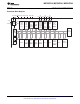
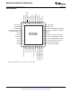
MSP430F5342, MSP430F5341, MSP430F5340 SLAS706E – JULY 2011 – REVISED AUGUST 2013 www.ti.com P5.7/TB0.1 DVSS3 P5.2/XT2IN P5.3/XT2OUT TEST/SBWTCK PJ.0/TDO PJ.1/TDI/TCLK PJ.2/TMS PJ.3/TCK RST/NMI/SBWTDIO P6.1/CB1/A1 P6.2/CB2/A2 Pin Designation 48 47 46 45 44 43 42 41 40 39 38 37 P6.3/CB3/A3 1 36 P4.7/PM_NONE P6.4/CB4/A4 2 35 P4.6/PM_NONE P6.5/CB5/A5 3 34 P4.5/PM_UCA1RXD/PM_UCA1SOMI P5.0/VREF+/VeREF+/A8 4 33 P4.4/PM_UCA1TXD/PM_UCA1SIMO P5.
MSP430F5342, MSP430F5341, MSP430F5340 www.ti.com SLAS706E – JULY 2011 – REVISED AUGUST 2013 Table 2. Terminal Functions TERMINAL NAME NO. I/O (1) DESCRIPTION P6.3/CB3/A3 1 I/O General-purpose digital I/O Comparator_B input CB3 Analog input A3 – ADC P6.4/CB4/A4 2 I/O General-purpose digital I/O Comparator_B input CB4 Analog input A4 – ADC P6.
MSP430F5342, MSP430F5341, MSP430F5340 SLAS706E – JULY 2011 – REVISED AUGUST 2013 www.ti.com Table 2. Terminal Functions (continued) TERMINAL NAME P1.7/TA1.0 NO. 20 I/O (1) DESCRIPTION I/O General-purpose digital I/O with port interrupt TA1 CCR0 capture: CCI0A input, compare: Out0 output P2.7/UCB0STE/UCA0CLK 21 I/O General-purpose digital I/O with port interrupt Slave transmit enable – USCI_B0 SPI mode Clock signal input – USCI_A0 SPI slave mode Clock signal output – USCI_A0 SPI master mode P3.
MSP430F5342, MSP430F5341, MSP430F5340 www.ti.com SLAS706E – JULY 2011 – REVISED AUGUST 2013 Table 2. Terminal Functions (continued) TERMINAL NAME NO. I/O (1) DESCRIPTION P4.7/PM_NONE 36 I/O General-purpose digital I/O with reconfigurable port mapping secondary function Default mapping: no secondary function. P5.7/TB0.1 37 I/O General-purpose digital I/O TB0 CCR1 capture: CCI1A input, compare: Out1 output DVSS3 38 P5.
MSP430F5342, MSP430F5341, MSP430F5340 SLAS706E – JULY 2011 – REVISED AUGUST 2013 www.ti.com Development Tools Support All MSP430™ microcontrollers are supported by a wide variety of software and hardware development tools. Tools are available from TI and various third parties. See them all at www.ti.com/msp430tools. Hardware Features See the Code Composer Studio for MSP430 User's Guide (SLAU157) for details on the available features.
MSP430F5342, MSP430F5341, MSP430F5340 www.ti.com SLAS706E – JULY 2011 – REVISED AUGUST 2013 SYS/BIOS SYS/BIOS is an advanced real-time operating system for the MSP430 microcontrollers. It features preemptive deterministic multi-tasking, hardware abstraction, memory management, and real-time analysis. SYS/BIOS is available free of charge and is provided with full source code.
MSP430F5342, MSP430F5341, MSP430F5340 SLAS706E – JULY 2011 – REVISED AUGUST 2013 www.ti.
MSP430F5342, MSP430F5341, MSP430F5340 www.ti.com SLAS706E – JULY 2011 – REVISED AUGUST 2013 Short-Form Description CPU The MSP430 CPU has a 16-bit RISC architecture that is highly transparent to the application. All operations, other than program-flow instructions, are performed as register operations in conjunction with seven addressing modes for source operand and four addressing modes for destination operand.
MSP430F5342, MSP430F5341, MSP430F5340 SLAS706E – JULY 2011 – REVISED AUGUST 2013 www.ti.com Interrupt Vector Addresses The interrupt vectors and the power-up start address are located in the address range 0FFFFh to 0FF80h. The vector contains the 16-bit address of the appropriate interrupt-handler instruction sequence. Table 3.
MSP430F5342, MSP430F5341, MSP430F5340 www.ti.com SLAS706E – JULY 2011 – REVISED AUGUST 2013 Table 3. Interrupt Sources, Flags, and Vectors (continued) (5) INTERRUPT SOURCE INTERRUPT FLAG Reserved Reserved (5) SYSTEM INTERRUPT WORD ADDRESS PRIORITY 0FFD0h 40 ⋮ ⋮ 0FF80h 0, lowest Reserved interrupt vectors at addresses are not used in this device and can be used for regular program code if necessary. To maintain compatibility with other devices, it is recommended to reserve these locations.
MSP430F5342, MSP430F5341, MSP430F5340 SLAS706E – JULY 2011 – REVISED AUGUST 2013 www.ti.com Bootstrap Loader (BSL) The BSL enables users to program the flash memory or RAM using a UART serial interface. Access to the device memory via the BSL is protected by an user-defined password. Usage of the BSL requires four pins as shown in Table 5. BSL entry requires a specific entry sequence on the RST/NMI/SBWTDIO and TEST/SBWTCK pins.
MSP430F5342, MSP430F5341, MSP430F5340 www.ti.com SLAS706E – JULY 2011 – REVISED AUGUST 2013 Spy-Bi-Wire Interface In addition to the standard JTAG interface, the MSP430 family supports the two wire Spy-Bi-Wire interface. SpyBi-Wire can be used to interface with MSP430 development tools and device programmers. The Spy-Bi-Wire interface pin requirements are shown in Table 7. For further details on interfacing to development tools and device programmers, see the MSP430 Hardware Tools User's Guide (SLAU278).
MSP430F5342, MSP430F5341, MSP430F5340 SLAS706E – JULY 2011 – REVISED AUGUST 2013 www.ti.com Port Mapping Controller The port mapping controller allows the flexible and reconfigurable mapping of digital functions to port P4. Table 8.
MSP430F5342, MSP430F5341, MSP430F5340 www.ti.com SLAS706E – JULY 2011 – REVISED AUGUST 2013 Table 9. Default Mapping PIN PxMAPy MNEMONIC INPUT PIN FUNCTION OUTPUT PIN FUNCTION P4.0/P4MAP0 PM_UCB1STE/PM_UCA1CLK USCI_B1 SPI slave transmit enable (direction controlled by USCI) USCI_A1 clock input/output (direction controlled by USCI) P4.1/P4MAP1 PM_UCB1SIMO/PM_UCB1SDA USCI_B1 SPI slave in master out (direction controlled by USCI) USCI_B1 I2C data (open drain and direction controlled by USCI) P4.
MSP430F5342, MSP430F5341, MSP430F5340 SLAS706E – JULY 2011 – REVISED AUGUST 2013 www.ti.com Real-Time Clock (RTC_A) The RTC_A module can be used as a general-purpose 32-bit counter (counter mode) or as an integrated realtime clock (RTC) (calendar mode). In counter mode, the RTC_A also includes two independent 8-bit timers that can be cascaded to form a 16-bit timer/counter. Both timers can be read and written by software.
MSP430F5342, MSP430F5341, MSP430F5340 www.ti.com SLAS706E – JULY 2011 – REVISED AUGUST 2013 Table 10. System Module Interrupt Vector Registers (continued) INTERRUPT VECTOR REGISTER ADDRESS INTERRUPT EVENT VALUE SYSUNIV, User NMI 019Ah No interrupt pending 00h NMIFG 02h OFIFG 04h ACCVIFG 06h Reserved 08h Reserved 0Ah to 1Eh PRIORITY Highest Lowest DMA Controller The DMA controller allows movement of data from one memory address to another without CPU intervention.
MSP430F5342, MSP430F5341, MSP430F5340 SLAS706E – JULY 2011 – REVISED AUGUST 2013 www.ti.com Table 11. DMA Trigger Assignments(1) (continued) CHANNEL TRIGGER 0 1 2 30 DMA2IFG DMA0IFG DMA1IFG 31 DMAE0 DMAE0 DMAE0 Universal Serial Communication Interface (USCI) The USCI modules are used for serial data communication.
MSP430F5342, MSP430F5341, MSP430F5340 www.ti.com SLAS706E – JULY 2011 – REVISED AUGUST 2013 TA1 TA1 is a 16-bit timer/counter (Timer_A type) with three capture/compare registers. It can support multiple captures or compares, PWM outputs, and interval timing. It also has extensive interrupt capabilities. Interrupts may be generated from the counter on overflow conditions and from each of the capture/compare registers. Table 13. TA1 Signal Connections INPUT PIN NUMBER 19-P1.
MSP430F5342, MSP430F5341, MSP430F5340 SLAS706E – JULY 2011 – REVISED AUGUST 2013 www.ti.com TB0 TB0 is a 16-bit timer/counter (Timer_B type) with seven capture/compare registers. It can support multiple captures or compares, PWM outputs, and interval timing. It also has extensive interrupt capabilities. Interrupts may be generated from the counter on overflow conditions and from each of the capture/compare registers. Table 15. TB0 Signal Connections INPUT PIN NUMBER (1) 37-P5.
MSP430F5342, MSP430F5341, MSP430F5340 www.ti.com SLAS706E – JULY 2011 – REVISED AUGUST 2013 Comparator_B The primary function of the Comparator_B module is to support precision slope analog-to-digital conversions, battery voltage supervision, and monitoring of external analog signals. ADC12_A The ADC12_A module supports fast, 12-bit analog-to-digital conversions. The module implements a 12-bit SAR core, sample select control, reference generator and a 16 word conversion-and-control buffer.
MSP430F5342, MSP430F5341, MSP430F5340 SLAS706E – JULY 2011 – REVISED AUGUST 2013 www.ti.com Peripheral File Map Table 16.
MSP430F5342, MSP430F5341, MSP430F5340 www.ti.com SLAS706E – JULY 2011 – REVISED AUGUST 2013 Table 17. Special Function Registers (Base Address: 0100h) REGISTER DESCRIPTION REGISTER OFFSET SFR interrupt enable SFRIE1 00h SFR interrupt flag SFRIFG1 02h SFR reset pin control SFRRPCR 04h Table 18.
MSP430F5342, MSP430F5341, MSP430F5340 SLAS706E – JULY 2011 – REVISED AUGUST 2013 www.ti.com Table 24.
MSP430F5342, MSP430F5341, MSP430F5340 www.ti.com SLAS706E – JULY 2011 – REVISED AUGUST 2013 Table 27.
MSP430F5342, MSP430F5341, MSP430F5340 SLAS706E – JULY 2011 – REVISED AUGUST 2013 www.ti.com Table 29.
MSP430F5342, MSP430F5341, MSP430F5340 www.ti.com SLAS706E – JULY 2011 – REVISED AUGUST 2013 Table 32.
MSP430F5342, MSP430F5341, MSP430F5340 SLAS706E – JULY 2011 – REVISED AUGUST 2013 www.ti.com Table 35.
MSP430F5342, MSP430F5341, MSP430F5340 www.ti.com SLAS706E – JULY 2011 – REVISED AUGUST 2013 Table 36.
MSP430F5342, MSP430F5341, MSP430F5340 SLAS706E – JULY 2011 – REVISED AUGUST 2013 www.ti.com Table 37.
MSP430F5342, MSP430F5341, MSP430F5340 www.ti.com SLAS706E – JULY 2011 – REVISED AUGUST 2013 Table 39.
MSP430F5342, MSP430F5341, MSP430F5340 SLAS706E – JULY 2011 – REVISED AUGUST 2013 www.ti.com Table 42.
MSP430F5342, MSP430F5341, MSP430F5340 www.ti.com SLAS706E – JULY 2011 – REVISED AUGUST 2013 Table 43.
MSP430F5342, MSP430F5341, MSP430F5340 SLAS706E – JULY 2011 – REVISED AUGUST 2013 www.ti.com Absolute Maximum Ratings (1) over operating free-air temperature range (unless otherwise noted) Voltage applied at VCC to VSS -0.3 V to 4.1 V Voltage applied to any pin (excluding VCORE) (2) -0.3 V to VCC + 0.
MSP430F5342, MSP430F5341, MSP430F5340 www.ti.com SLAS706E – JULY 2011 – REVISED AUGUST 2013 Recommended Operating Conditions Typical values are specified at VCC = 3.3 V and TA = 25°C (unless otherwise noted) MIN Supply voltage during program execution and flash programming (AVCCx = DVCCx = VCC) (1) (2) VCC NOM MAX UNIT PMMCOREVx = 0 1.8 3.6 V PMMCOREVx = 0, 1 2.0 3.6 V PMMCOREVx = 0, 1, 2 2.2 3.6 V PMMCOREVx = 0, 1, 2, 3 2.4 3.
MSP430F5342, MSP430F5341, MSP430F5340 SLAS706E – JULY 2011 – REVISED AUGUST 2013 www.ti.com Electrical Characteristics Active Mode Supply Current Into VCC Excluding External Current over recommended operating free-air temperature (unless otherwise noted) (1) (2) (3) FREQUENCY (fDCO = fMCLK = fSMCLK) PARAMETER IAM, IAM, (1) (2) (3) 38 Flash RAM EXECUTION MEMORY Flash RAM VCC 3V 3V PMMCOREVx 1 MHz 8 MHz 12 MHz TYP MAX 2.65 4.0 4.4 2.90 20 MHz TYP MAX TYP MAX 0 0.36 0.47 2.
MSP430F5342, MSP430F5341, MSP430F5340 www.ti.com SLAS706E – JULY 2011 – REVISED AUGUST 2013 Low-Power Mode Supply Currents (Into VCC) Excluding External Current over recommended ranges of supply voltage and operating free-air temperature (unless otherwise noted) (1) PARAMETER ILPM0,1MHz Low-power mode 0 (3) (4) ILPM2 Low-power mode 2 (5) (4) ILPM4 0 73 77 85 80 85 97 3V 3 79 83 92 88 95 105 2.2 V 0 6.5 6.5 12 10 11 17 3V 3 7.0 7.0 13 11 12 18 0 1.60 1.90 2.6 5.
MSP430F5342, MSP430F5341, MSP430F5340 SLAS706E – JULY 2011 – REVISED AUGUST 2013 www.ti.com Schmitt-Trigger Inputs – General Purpose I/O (1) (P1.0 to P1.7, P2.7, P3.0 to P3.4, P4.0 to P4.7) (P5.0 to P5.5, P5.7, P6.1 to P6.5, PJ.0 to PJ.
MSP430F5342, MSP430F5341, MSP430F5340 www.ti.com SLAS706E – JULY 2011 – REVISED AUGUST 2013 Outputs – General Purpose I/O (Full Drive Strength) (P1.0 to P1.7, P2.7, P3.0 to P3.4, P4.0 to P4.7) (P5.0 to P5.5, P5.7, P6.1 to P6.5, PJ.0 to PJ.3) over recommended ranges of supply voltage and operating free-air temperature (unless otherwise noted) PARAMETER TEST CONDITIONS I(OHmax) = -3 mA (1) VOH 1.
MSP430F5342, MSP430F5341, MSP430F5340 SLAS706E – JULY 2011 – REVISED AUGUST 2013 www.ti.com Typical Characteristics – Outputs, Reduced Drive Strength (PxDS.y = 0) over recommended ranges of supply voltage and operating free-air temperature (unless otherwise noted) TYPICAL LOW-LEVEL OUTPUT CURRENT vs LOW-LEVEL OUTPUT VOLTAGE TYPICAL LOW-LEVEL OUTPUT CURRENT vs LOW-LEVEL OUTPUT VOLTAGE 8.0 VCC = 3.0 V Px.y IOL – Typical Low-Level Output Current – mA IOL – Typical Low-Level Output Current – mA 25.
MSP430F5342, MSP430F5341, MSP430F5340 www.ti.com SLAS706E – JULY 2011 – REVISED AUGUST 2013 Typical Characteristics – Outputs, Full Drive Strength (PxDS.y = 1) over recommended ranges of supply voltage and operating free-air temperature (unless otherwise noted) TYPICAL LOW-LEVEL OUTPUT CURRENT vs LOW-LEVEL OUTPUT VOLTAGE TA = 25°C VCC = 3.0 V Px.y 55.0 50.0 IOL – Typical Low-Level Output Current – mA IOL – Typical Low-Level Output Current – mA 60.
MSP430F5342, MSP430F5341, MSP430F5340 SLAS706E – JULY 2011 – REVISED AUGUST 2013 www.ti.com Crystal Oscillator, XT1, Low-Frequency Mode (1) over recommended ranges of supply voltage and operating free-air temperature (unless otherwise noted) PARAMETER TEST CONDITIONS VCC MIN fOSC = 32768 Hz, XTS = 0, XT1BYPASS = 0, XT1DRIVEx = 1, TA = 25°C ΔIDVCC.
MSP430F5342, MSP430F5341, MSP430F5340 www.ti.com SLAS706E – JULY 2011 – REVISED AUGUST 2013 Crystal Oscillator, XT2 over recommended ranges of supply voltage and operating free-air temperature (unless otherwise noted) (1) PARAMETER TEST CONDITIONS VCC MIN fOSC = 4 MHz, XT2OFF = 0, XT2BYPASS = 0, XT2DRIVEx = 0, TA = 25°C IDVCC.
MSP430F5342, MSP430F5341, MSP430F5340 SLAS706E – JULY 2011 – REVISED AUGUST 2013 www.ti.com Internal Very-Low-Power Low-Frequency Oscillator (VLO) over recommended ranges of supply voltage and operating free-air temperature (unless otherwise noted) PARAMETER TEST CONDITIONS VCC fVLO VLO frequency Measured at ACLK 1.8 V to 3.6 V dfVLO/dT VLO frequency temperature drift Measured at ACLK (1) 1.8 V to 3.6 V Measured at ACLK (2) 1.8 V to 3.6 V Measured at ACLK 1.8 V to 3.
MSP430F5342, MSP430F5341, MSP430F5340 www.ti.com SLAS706E – JULY 2011 – REVISED AUGUST 2013 DCO Frequency over recommended ranges of supply voltage and operating free-air temperature (unless otherwise noted) PARAMETER TEST CONDITIONS (1) MIN TYP MAX UNIT fDCO(0,0) DCO frequency (0, 0) DCORSELx = 0, DCOx = 0, MODx = 0 0.07 0.20 MHz fDCO(0,31) DCO frequency (0, 31) (1) DCORSELx = 0, DCOx = 31, MODx = 0 0.70 1.70 MHz fDCO(1,0) DCO frequency (1, 0) (1) DCORSELx = 1, DCOx = 0, MODx = 0 0.
MSP430F5342, MSP430F5341, MSP430F5340 SLAS706E – JULY 2011 – REVISED AUGUST 2013 www.ti.
MSP430F5342, MSP430F5341, MSP430F5340 www.ti.com SLAS706E – JULY 2011 – REVISED AUGUST 2013 PMM, SVS High Side over recommended ranges of supply voltage and operating free-air temperature (unless otherwise noted) PARAMETER TEST CONDITIONS MIN SVSHE = 0, DVCC = 3.
MSP430F5342, MSP430F5341, MSP430F5340 SLAS706E – JULY 2011 – REVISED AUGUST 2013 www.ti.com PMM, SVM High Side over recommended ranges of supply voltage and operating free-air temperature (unless otherwise noted) PARAMETER TEST CONDITIONS MIN TYP SVMHE = 0, DVCC = 3.6 V I(SVMH) SVMH current consumption V(SVMH) SVMH on or off voltage level (1) 0 t(SVMH) (1) SVMH propagation delay SVMH on or off delay time UNIT nA SVMHE= 1, DVCC = 3.6 V, SVMHFP = 0 200 nA SVMHE = 1, DVCC = 3.
MSP430F5342, MSP430F5341, MSP430F5340 www.ti.com SLAS706E – JULY 2011 – REVISED AUGUST 2013 Wake Up From Low Power Modes and Reset over recommended ranges of supply voltage and operating free-air temperature (unless otherwise noted) PARAMETER TEST CONDITIONS MIN TYP MAX UNIT fMCLK ≥ 4.0 MHz 3.5 7.5 1.0 MHz < fMCLK < 4.0 MHz 4.
MSP430F5342, MSP430F5341, MSP430F5340 SLAS706E – JULY 2011 – REVISED AUGUST 2013 www.ti.
MSP430F5342, MSP430F5341, MSP430F5340 www.ti.com SLAS706E – JULY 2011 – REVISED AUGUST 2013 1/fUCxCLK CKPL = 0 UCLK CKPL = 1 tLO/HI tLO/HI tSU,MI tHD,MI SOMI tHD,MO tVALID,MO SIMO Figure 12. SPI Master Mode, CKPH = 0 1/fUCxCLK CKPL = 0 UCLK CKPL = 1 tLO/HI tLO/HI tSU,MI tHD,MI SOMI tHD,MO tVALID,MO SIMO Figure 13.
MSP430F5342, MSP430F5341, MSP430F5340 SLAS706E – JULY 2011 – REVISED AUGUST 2013 www.ti.
MSP430F5342, MSP430F5341, MSP430F5340 www.ti.com SLAS706E – JULY 2011 – REVISED AUGUST 2013 tSTE,LEAD tSTE,LAG STE 1/fUCxCLK CKPL = 0 UCLK CKPL = 1 tLO/HI tSU,SI tLO/HI tHD,SI SIMO tHD,SO tVALID,SO tSTE,ACC tSTE,DIS SOMI Figure 14. SPI Slave Mode, CKPH = 0 tSTE,LAG tSTE,LEAD STE 1/fUCxCLK CKPL = 0 UCLK CKPL = 1 tLO/HI tLO/HI tHD,SI tSU,SI SIMO tSTE,ACC tHD,MO tVALID,SO tSTE,DIS SOMI Figure 15.
MSP430F5342, MSP430F5341, MSP430F5340 SLAS706E – JULY 2011 – REVISED AUGUST 2013 www.ti.
MSP430F5342, MSP430F5341, MSP430F5340 www.ti.
MSP430F5342, MSP430F5341, MSP430F5340 SLAS706E – JULY 2011 – REVISED AUGUST 2013 www.ti.com 12-Bit ADC, Linearity Parameters Using an External Reference Voltage or AVCC as Reference Voltage over recommended ranges of supply voltage and operating free-air temperature (unless otherwise noted) PARAMETER TEST CONDITIONS 1.4 V ≤ dVREF ≤ 1.6 V (2) EI Integral linearity error (1) ED Differential linearity error (1) EO Offset error (3) EG Gain error (3) ET (1) (2) (3) 1.
MSP430F5342, MSP430F5341, MSP430F5340 www.ti.
MSP430F5342, MSP430F5341, MSP430F5340 SLAS706E – JULY 2011 – REVISED AUGUST 2013 www.ti.com REF, External Reference over recommended ranges of supply voltage and operating free-air temperature (unless otherwise noted) (1) PARAMETER TEST CONDITIONS VCC MIN TYP MAX UNIT VeREF+ Positive external reference voltage input VeREF+ > VREF-/VeREF- (2) 1.4 AVCC V VREF-/VeREF- Negative external reference voltage input VeREF+ > VREF-/VeREF- (3) 0 1.
MSP430F5342, MSP430F5341, MSP430F5340 www.ti.com SLAS706E – JULY 2011 – REVISED AUGUST 2013 REF, Built-In Reference over recommended ranges of supply voltage and operating free-air temperature (unless otherwise noted) (1) PARAMETER VREF+ AVCC(min) IREF+ TEST CONDITIONS Positive built-in reference voltage output AVCC minimum voltage, Positive built-in reference active Operating supply current into AVCC terminal (2) (3) VCC MIN REFVSEL = {2} for 2.5 V, REFON = REFOUT = 1, IVREF+= 0 A 3V 2.
MSP430F5342, MSP430F5341, MSP430F5340 SLAS706E – JULY 2011 – REVISED AUGUST 2013 www.ti.com Comparator B over recommended ranges of supply voltage and operating free-air temperature (unless otherwise noted) PARAMETER VCC TEST CONDITIONS VCC Supply voltage MIN TYP 1.8 3.6 1.
MSP430F5342, MSP430F5341, MSP430F5340 www.ti.com SLAS706E – JULY 2011 – REVISED AUGUST 2013 Flash Memory over recommended ranges of supply voltage and operating free-air temperature (unless otherwise noted) TEST CONDITIONS PARAMETER DVCC(PGM/ERASE) Program or erase supply voltage MIN TYP 1.8 MAX 3.
MSP430F5342, MSP430F5341, MSP430F5340 SLAS706E – JULY 2011 – REVISED AUGUST 2013 www.ti.com INPUT/OUTPUT SCHEMATICS Port P1, P1.0 to P1.7, Input/Output With Schmitt Trigger Pad Logic P1REN.x P1DIR.x 0 From module 1 P1OUT.x 0 From module 1 DVSS 0 DVCC 1 Direction 0: Input 1: Output P1DS.x 0: Low drive 1: High drive P1SEL.x P1IN.x EN To module 1 P1.0/TA0CLK/ACLK P1.1/TA0.0 P1.2/TA0.1 P1.3/TA0.2 P1.4/TA0.3 P1.5/TA0.4 P1.6/TA1CLK/CBOUT P1.7/TA1.0 D P1IE.x EN P1IRQ.x Q P1IFG.
MSP430F5342, MSP430F5341, MSP430F5340 www.ti.com SLAS706E – JULY 2011 – REVISED AUGUST 2013 Table 44. Port P1 (P1.0 to P1.7) Pin Functions PIN NAME (P1.x) P1.0/TA0CLK/ACLK P1.1/TA0.0 P1.2/TA0.1 P1.3/TA0.2 P1.4/TA0.3 x 0 1 2 3 4 CONTROL BITS/SIGNALS FUNCTION P1DIR.x P1SEL.x P1.0 (I/O) I: 0; O: 1 0 TA0CLK 0 1 ACLK 1 1 I: 0; O: 1 0 TA0.CCI0A 0 1 TA0.0 1 1 I: 0; O: 1 0 TA0.CCI1A 0 1 TA0.1 1 1 I: 0; O: 1 0 TA0.CCI2A 0 1 TA0.2 1 1 I: 0; O: 1 0 0 1 P1.
MSP430F5342, MSP430F5341, MSP430F5340 SLAS706E – JULY 2011 – REVISED AUGUST 2013 www.ti.com Port P2, P2.7, Input/Output With Schmitt Trigger Pad Logic P2REN.x P2DIR.x 0 From module 1 P2OUT.x 0 From module 1 DVSS 0 DVCC 1 1 Direction 0: Input 1: Output P2.7/UB0STE/UCA0CLK P2DS.x 0: Low drive 1: High drive P2SEL.x P2IN.x EN To module D P2IE.x EN To module Q P2IFG.x Set P2SEL.x Interrupt Edge Select P2IES.x Table 45. Port P2 (P2.7) Pin Functions PIN NAME (P2.x) P2.
MSP430F5342, MSP430F5341, MSP430F5340 www.ti.com SLAS706E – JULY 2011 – REVISED AUGUST 2013 Port P3, P3.0 to P3.4, Input/Output With Schmitt Trigger Pad Logic P3REN.x P3DIR.x 0 From module 1 P3OUT.x 0 From module 1 DVSS 0 DVCC 1 1 Direction 0: Input 1: Output P3.0/UCB0SIMO/UCB0SDA P3.1/UCB0SOMI/UCB0SCL P3.2/UCB0CLK/UCA0STE P3.3/UCA0TXD/UCA0SIMO P3.4/UCA0RXD/UCA0SOMI P3DS.x 0: Low drive 1: High drive P3SEL.x P3IN.x EN To module D Table 46. Port P3 (P3.0 to P3.
MSP430F5342, MSP430F5341, MSP430F5340 SLAS706E – JULY 2011 – REVISED AUGUST 2013 www.ti.com Port P4, P4.0 to P4.7, Input/Output With Schmitt Trigger Pad Logic P4REN.x P4DIR.x 0 from Port Mapping Control 1 P4OUT.x 0 from Port Mapping Control 1 DVSS 0 DVCC 1 1 Direction 0: Input 1: Output P4.0/P4MAP0 P4.1/P4MAP1 P4.2/P4MAP2 P4.3/P4MAP3 P4.4/P4MAP4 P4.5/P4MAP5 P4.6/P4MAP6 P4.7/P4MAP7 P4DS.x 0: Low drive 1: High drive P4SEL.x P4IN.x EN D to Port Mapping Control Table 47. Port P4 (P4.
MSP430F5342, MSP430F5341, MSP430F5340 www.ti.com SLAS706E – JULY 2011 – REVISED AUGUST 2013 Port P5, P5.0 and P5.1, Input/Output With Schmitt Trigger Pad Logic to/from Reference to ADC12 INCHx = x P5REN.x P5DIR.x DVSS 0 DVCC 1 1 0 1 P5OUT.x 0 From module 1 P5.0/A8/VREF+/VeREF+ P5.1/A9/VREF–/VeREF– P5DS.x 0: Low drive 1: High drive P5SEL.x P5IN.x Bus Keeper EN To module D Table 48. Port P5 (P5.0 and P5.1) Pin Functions PIN NAME (P5.x) P5.0/A8/VREF+/VeREF+ P5.
MSP430F5342, MSP430F5341, MSP430F5340 SLAS706E – JULY 2011 – REVISED AUGUST 2013 www.ti.com Port P5, P5.2, Input/Output With Schmitt Trigger Pad Logic To XT2 P5REN.2 P5DIR.2 DVSS 0 DVCC 1 1 0 1 P5OUT.2 0 Module X OUT 1 P5DS.2 0: Low drive 1: High drive P5SEL.2 P5.2/XT2IN P5IN.
MSP430F5342, MSP430F5341, MSP430F5340 www.ti.com SLAS706E – JULY 2011 – REVISED AUGUST 2013 Port P5, P5.3, Input/Output With Schmitt Trigger Pad Logic To XT2 P5REN.3 P5DIR.3 DVSS 0 DVCC 1 1 0 1 P5OUT.3 0 Module X OUT 1 P5.3/XT2OUT P5DS.3 0: Low drive 1: High drive P5SEL.3 P5IN.3 Bus Keeper EN Module X IN D Table 49. Port P5 (P5.2, P5.3) Pin Functions PIN NAME (P5.x) P5.2/XT2IN P5.3/XT2OUT (1) (2) (3) x 2 3 FUNCTION P5.2 (I/O) CONTROL BITS/SIGNALS (1) P5DIR.x P5SEL.2 P5SEL.
MSP430F5342, MSP430F5341, MSP430F5340 SLAS706E – JULY 2011 – REVISED AUGUST 2013 www.ti.com Port P5, P5.4 and P5.5 Input/Output With Schmitt Trigger Pad Logic to XT1 P5REN.4 P5DIR.4 DVSS 0 DVCC 1 1 0 1 P5OUT.4 0 Module X OUT 1 P5DS.4 0: Low drive 1: High drive P5SEL.4 P5.4/XIN P5IN.
MSP430F5342, MSP430F5341, MSP430F5340 www.ti.com SLAS706E – JULY 2011 – REVISED AUGUST 2013 Pad Logic to XT1 P5REN.5 P5DIR.5 DVSS 0 DVCC 1 1 0 1 P5OUT.5 0 Module X OUT 1 P5.5/XOUT P5DS.5 0: Low drive 1: High drive P5SEL.5 XT1BYPASS P5IN.5 Bus Keeper EN Module X IN D Table 50. Port P5 (P5.4 and P5.5) Pin Functions PIN NAME (P5.x) P5.4/XIN x 4 FUNCTION P5DIR.x P5SEL.4 P5SEL.
MSP430F5342, MSP430F5341, MSP430F5340 SLAS706E – JULY 2011 – REVISED AUGUST 2013 www.ti.com Port P5, P5.7, Input/Output With Schmitt Trigger Pad Logic P5REN.x P5DIR.x 0 From Module 1 P5OUT.x 0 DVSS 0 DVCC 1 1 Direction 0: Input 1: Output 1 P5.7/TB0.1 P5DS.x 0: Low drive 1: High drive P5SEL.x P5IN.x EN D To module Table 51. Port P5 (P5.7) Pin Functions PIN NAME (P5.x) P5.7/TB0.1 74 x 7 CONTROL BITS/SIGNALS FUNCTION P5DIR.x P5SEL.x TB0.CCI1A 0 1 TB0.
MSP430F5342, MSP430F5341, MSP430F5340 www.ti.com SLAS706E – JULY 2011 – REVISED AUGUST 2013 Port P6, P6.1 to P6.5, Input/Output With Schmitt Trigger Pad Logic to ADC12 INCHx = x to Comparator_B from Comparator_B CBPD.x P6REN.x P6DIR.x 0 0 From module 1 0 DVCC 1 1 Direction 0: Input 1: Output 1 P6OUT.x DVSS P6.1/CB1/A1 P6.2/CB2/A2 P6.3/CB3/A3 P6.4/CB4/A4 P6.5/CB5/A5 P6DS.x 0: Low drive 1: High drive P6SEL.x P6IN.x Bus Keeper EN D To module Table 52. Port P6 (P6.1 to P6.
MSP430F5342, MSP430F5341, MSP430F5340 SLAS706E – JULY 2011 – REVISED AUGUST 2013 www.ti.com Table 52. Port P6 (P6.1 to P6.5) Pin Functions (continued) PIN NAME (P6.x) P6.4/CB4/A4 P6.5/CB5/A5 76 x 4 5 FUNCTION P6.4 (I/O) CONTROL BITS/SIGNALS (1) P6DIR.x P6SEL.x CBPD I: 0; O: 1 0 0 A4 X 1 X CB4 (2) X X 1 P6.
MSP430F5342, MSP430F5341, MSP430F5340 www.ti.com SLAS706E – JULY 2011 – REVISED AUGUST 2013 Port J, J.0 JTAG pin TDO, Input/Output With Schmitt Trigger or Output Pad Logic PJREN.0 PJDIR.0 0 DVCC 1 PJOUT.0 0 From JTAG 1 DVSS 0 DVCC 1 1 PJ.0/TDO PJDS.0 0: Low drive 1: High drive From JTAG PJIN.0 EN D Port J, J.1 to J.3 JTAG pins TMS, TCK, TDI/TCLK, Input/Output With Schmitt Trigger or Output Pad Logic PJREN.x PJDIR.x 0 DVSS 1 PJOUT.x 0 From JTAG 1 DVSS 0 DVCC 1 1 PJDS.
MSP430F5342, MSP430F5341, MSP430F5340 SLAS706E – JULY 2011 – REVISED AUGUST 2013 www.ti.com Table 53. Port PJ (PJ.0 to PJ.3) Pin Functions PIN NAME (PJ.x) x CONTROL BITS/ SIGNALS (1) FUNCTION PJDIR.x PJ.0/TDO 0 (2) I: 0; O: 1 PJ.1 (I/O) (2) I: 0; O: 1 PJ.0 (I/O) TDO (3) PJ.1/TDI/TCLK 1 X TDI/TCLK (3) PJ.2/TMS 2 PJ.2 (I/O) TMS (3) PJ.3/TCK 3 (1) (2) (3) (4) 78 X I: 0; O: 1 (4) PJ.
MSP430F5342, MSP430F5341, MSP430F5340 www.ti.com SLAS706E – JULY 2011 – REVISED AUGUST 2013 DEVICE DESCRIPTORS Table 54 lists the complete contents of the device descriptor tag-length-value (TLV) structure for each device type. Table 54.
MSP430F5342, MSP430F5341, MSP430F5340 SLAS706E – JULY 2011 – REVISED AUGUST 2013 www.ti.com Table 54.
MSP430F5342, MSP430F5341, MSP430F5340 www.ti.com SLAS706E – JULY 2011 – REVISED AUGUST 2013 Table 54.
MSP430F5342, MSP430F5341, MSP430F5340 SLAS706E – JULY 2011 – REVISED AUGUST 2013 www.ti.com REVISION HISTORY REVISION SLAS706 82 DESCRIPTION Product Preview release SLAS706A Updated Product Preview release SLAS706B Production Data release SLAS706C Pinout and Terminal Functions, Added recommendation to connect exposed thermal pad to VSS. Terminal Functions, Changed ACLK description (added dividers up to 32). Table 10, Changed SYSRSTIV interrupt event at 1Ch to Reserved.
PACKAGE OPTION ADDENDUM www.ti.
PACKAGE OPTION ADDENDUM www.ti.com 5-Jul-2013 Important Information and Disclaimer:The information provided on this page represents TI's knowledge and belief as of the date that it is provided. TI bases its knowledge and belief on information provided by third parties, and makes no representation or warranty as to the accuracy of such information. Efforts are underway to better integrate information from third parties.
IMPORTANT NOTICE Texas Instruments Incorporated and its subsidiaries (TI) reserve the right to make corrections, enhancements, improvements and other changes to its semiconductor products and services per JESD46, latest issue, and to discontinue any product or service per JESD48, latest issue. Buyers should obtain the latest relevant information before placing orders and should verify that such information is current and complete.