MSP430F5510, MSP430F5509, MSP430F5508, MSP430F5507 MSP430F5506, MSP430F5505, MSP430F5504, MSP430F5503 MSP430F5502, MSP430F5501, MSP430F5500 www.ti.com SLAS645I – JULY 2009 – REVISED NOVEMBER 2013 MSP430F5510, MSP430F550x Mixed Signal Microcontrollers Check for Samples: MSP430F5510, MSP430F5509, MSP430F5508, MSP430F5507, MSP430F5506, MSP430F5505, MSP430F5504, MSP430F5503, MSP430F5502, MSP430F5501, MSP430F5500 FEATURES 1 • 23 • • • • • Low Supply-Voltage Range: 3.6 V Down to 1.
MSP430F5510, MSP430F5509, MSP430F5508, MSP430F5507 MSP430F5506, MSP430F5505, MSP430F5504, MSP430F5503 MSP430F5502, MSP430F5501, MSP430F5500 SLAS645I – JULY 2009 – REVISED NOVEMBER 2013 • • Table 1 Summarizes Family Members For Complete Module Descriptions, See the MSP430x5xx and MSP430x6xx Family User's Guide (SLAU208) www.ti.
MSP430F5510, MSP430F5509, MSP430F5508, MSP430F5507 MSP430F5506, MSP430F5505, MSP430F5504, MSP430F5503 MSP430F5502, MSP430F5501, MSP430F5500 www.ti.com SLAS645I – JULY 2009 – REVISED NOVEMBER 2013 Table 1.
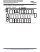
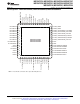
MSP430F5510, MSP430F5509, MSP430F5508, MSP430F5507 MSP430F5506, MSP430F5505, MSP430F5504, MSP430F5503 MSP430F5502, MSP430F5501, MSP430F5500 SLAS645I – JULY 2009 – REVISED NOVEMBER 2013 www.ti.com Functional Block Diagram – MSP430F5510IRGC, MSP430F5509IRGC, MSP430F5508IRGC, MSP430F5510IZQE, MSP430F5509IZQE, MSP430F5508IZQE XIN XOUT RST/NMI DVCC DVSS VCORE AVCC AVSS P1.
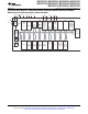
MSP430F5510, MSP430F5509, MSP430F5508, MSP430F5507 MSP430F5506, MSP430F5505, MSP430F5504, MSP430F5503 MSP430F5502, MSP430F5501, MSP430F5500 www.ti.com SLAS645I – JULY 2009 – REVISED NOVEMBER 2013 VSSU PU.0/DP PUR PU.1/DM VBUS VUSB V18 AVSS2 P5.2/XT2IN P5.3/XT2OUT TEST/SBWTCK PJ.0/TDO PJ.1/TDI/TCLK PJ.2/TMS PJ.3/TCK RST/NMI/SBWTDIO Pin Designation – MSP430F5510IRGC, MSP430F5509IRGC, MSP430F5508IRGC 64 63 62 61 60 59 58 57 56 55 54 53 52 51 50 49 P6.0/CB0/A0 1 48 P4.7/PM_NONE P6.
MSP430F5510, MSP430F5509, MSP430F5508, MSP430F5507 MSP430F5506, MSP430F5505, MSP430F5504, MSP430F5503 MSP430F5502, MSP430F5501, MSP430F5500 SLAS645I – JULY 2009 – REVISED NOVEMBER 2013 www.ti.
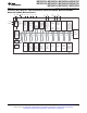
MSP430F5510, MSP430F5509, MSP430F5508, MSP430F5507 MSP430F5506, MSP430F5505, MSP430F5504, MSP430F5503 MSP430F5502, MSP430F5501, MSP430F5500 www.ti.com SLAS645I – JULY 2009 – REVISED NOVEMBER 2013 Functional Block Diagram – MSP430F5510IRGZ, MSP430F5509IRGZ, MSP430F5508IRGZ, MSP430F5510IPT, MSP430F5509IPT, MSP430F5508IPT XIN XOUT RST/NMI DVCC DVSS VCORE AVCC AVSS P1.
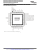
MSP430F5510, MSP430F5509, MSP430F5508, MSP430F5507 MSP430F5506, MSP430F5505, MSP430F5504, MSP430F5503 MSP430F5502, MSP430F5501, MSP430F5500 SLAS645I – JULY 2009 – REVISED NOVEMBER 2013 www.ti.com VSSU PU.0/DP PUR PU.1/DM VBUS VUSB V18 AVSS2 P5.2/XT2IN P5.3/XT2OUT TEST/SBWTCK RST/NMI/SBWTDIO Pin Designation – MSP430F5510IRGZ, MSP430F5509IRGZ, MSP430F5508IRGZ, MSP430F5510IPT, MSP430F5509IPT, MSP430F5508IPT 48 47 46 45 44 43 42 41 40 39 38 37 P6.0/CB0/A0 1 36 P4.7/PM_NONE P6.
MSP430F5510, MSP430F5509, MSP430F5508, MSP430F5507 MSP430F5506, MSP430F5505, MSP430F5504, MSP430F5503 MSP430F5502, MSP430F5501, MSP430F5500 www.ti.com SLAS645I – JULY 2009 – REVISED NOVEMBER 2013 Functional Block Diagram – MSP430F5507IRGZ, MSP430F5506IRGZ, MSP430F5505IRGZ, MSP430F5504IRGZ, MSP430F5504IPT XIN XOUT RST/NMI DVCC DVSS VCORE AVCC AVSS P1.
MSP430F5510, MSP430F5509, MSP430F5508, MSP430F5507 MSP430F5506, MSP430F5505, MSP430F5504, MSP430F5503 MSP430F5502, MSP430F5501, MSP430F5500 SLAS645I – JULY 2009 – REVISED NOVEMBER 2013 www.ti.com VSSU PU.0/DP PUR PU.1/DM VBUS VUSB V18 AVSS2 P5.2/XT2IN P5.3/XT2OUT TEST/SBWTCK RST/NMI/SBWTDIO Pin Designation – MSP430F5507IRGZ, MSP430F5506IRGZ, MSP430F5505IRGZ, MSP430F5504IRGZ, MSP430F5504IPT 48 47 46 45 44 43 42 41 40 39 38 37 P6.0/A0 1 36 P4.7/PM_NONE P6.1/A1 2 35 P4.6/PM_NONE P6.
MSP430F5510, MSP430F5509, MSP430F5508, MSP430F5507 MSP430F5506, MSP430F5505, MSP430F5504, MSP430F5503 MSP430F5502, MSP430F5501, MSP430F5500 www.ti.com SLAS645I – JULY 2009 – REVISED NOVEMBER 2013 Functional Block Diagram – MSP430F5503IRGZ, MSP430F5502IRGZ, MSP430F5501IRGZ, MSP430F5500IRGZ XIN XOUT RST/NMI DVCC DVSS VCORE AVCC AVSS P1.
MSP430F5510, MSP430F5509, MSP430F5508, MSP430F5507 MSP430F5506, MSP430F5505, MSP430F5504, MSP430F5503 MSP430F5502, MSP430F5501, MSP430F5500 SLAS645I – JULY 2009 – REVISED NOVEMBER 2013 www.ti.com VSSU PU.0/DP PUR PU.1/DM VBUS VUSB V18 AVSS2 P5.2/XT2IN P5.3/XT2OUT TEST/SBWTCK RST/NMI/SBWTDIO Pin Designation – MSP430F5503IRGZ, MSP430F5502IRGZ, MSP430F5501IRGZ, MSP430F5500IRGZ 48 47 46 45 44 43 42 41 40 39 38 37 P6.0/CB0 1 36 P4.7/PM_NONE P6.1/CB1 2 35 P4.6/PM_NONE P6.2/CB2 3 34 P4.
MSP430F5510, MSP430F5509, MSP430F5508, MSP430F5507 MSP430F5506, MSP430F5505, MSP430F5504, MSP430F5503 MSP430F5502, MSP430F5501, MSP430F5500 www.ti.com SLAS645I – JULY 2009 – REVISED NOVEMBER 2013 Table 2. Terminal Functions TERMINAL NO. NAME I/O (1) DESCRIPTION RGC RGZ, PT ZQE P6.4/CB4/A4 5 N/A C1 I/O General-purpose digital I/O Comparator_B input CB4 (not available on PT and RGZ package devices) Analog input A4 – ADC (not available on PT and RGZ package devices) P6.
MSP430F5510, MSP430F5509, MSP430F5508, MSP430F5507 MSP430F5506, MSP430F5505, MSP430F5504, MSP430F5503 MSP430F5502, MSP430F5501, MSP430F5500 SLAS645I – JULY 2009 – REVISED NOVEMBER 2013 www.ti.com Table 2. Terminal Functions (continued) TERMINAL NO. NAME I/O (1) DESCRIPTION RGC RGZ, PT ZQE P2.0/TA1.1 26 22 J5 I/O General-purpose digital I/O with port interrupt TA1 CCR1 capture: CCI1A input, compare: Out1 output P2.1/TA1.
MSP430F5510, MSP430F5509, MSP430F5508, MSP430F5507 MSP430F5506, MSP430F5505, MSP430F5504, MSP430F5503 MSP430F5502, MSP430F5501, MSP430F5500 www.ti.com SLAS645I – JULY 2009 – REVISED NOVEMBER 2013 Table 2. Terminal Functions (continued) TERMINAL NO. NAME P4.
MSP430F5510, MSP430F5509, MSP430F5508, MSP430F5507 MSP430F5506, MSP430F5505, MSP430F5504, MSP430F5503 MSP430F5502, MSP430F5501, MSP430F5500 SLAS645I – JULY 2009 – REVISED NOVEMBER 2013 www.ti.com Table 2. Terminal Functions (continued) TERMINAL NO. NAME P6.2/CB2/A2 P6.
MSP430F5510, MSP430F5509, MSP430F5508, MSP430F5507 MSP430F5506, MSP430F5505, MSP430F5504, MSP430F5503 MSP430F5502, MSP430F5501, MSP430F5500 www.ti.com SLAS645I – JULY 2009 – REVISED NOVEMBER 2013 Development Tools Support All MSP430™ microcontrollers are supported by a wide variety of software and hardware development tools. Tools are available from TI and various third parties. See them all at www.ti.com/msp430tools.
MSP430F5510, MSP430F5509, MSP430F5508, MSP430F5507 MSP430F5506, MSP430F5505, MSP430F5504, MSP430F5503 MSP430F5502, MSP430F5501, MSP430F5500 SLAS645I – JULY 2009 – REVISED NOVEMBER 2013 www.ti.com MSP430 USB Developer's Package MSP430 USB Developer's Package is an easy-to-use USB stack implementation for the MSP430 microcontrollers.
MSP430F5510, MSP430F5509, MSP430F5508, MSP430F5507 MSP430F5506, MSP430F5505, MSP430F5504, MSP430F5503 MSP430F5502, MSP430F5501, MSP430F5500 www.ti.
MSP430F5510, MSP430F5509, MSP430F5508, MSP430F5507 MSP430F5506, MSP430F5505, MSP430F5504, MSP430F5503 MSP430F5502, MSP430F5501, MSP430F5500 SLAS645I – JULY 2009 – REVISED NOVEMBER 2013 www.ti.com Short-Form Description CPU (Link to User's Guide) The MSP430 CPU has a 16-bit RISC architecture that is highly transparent to the application.
MSP430F5510, MSP430F5509, MSP430F5508, MSP430F5507 MSP430F5506, MSP430F5505, MSP430F5504, MSP430F5503 MSP430F5502, MSP430F5501, MSP430F5500 www.ti.com SLAS645I – JULY 2009 – REVISED NOVEMBER 2013 Interrupt Vector Addresses The interrupt vectors and the power-up start address are located in the address range 0FFFFh to 0FF80h. The vector contains the 16-bit address of the appropriate interrupt-handler instruction sequence. Table 3.
MSP430F5510, MSP430F5509, MSP430F5508, MSP430F5507 MSP430F5506, MSP430F5505, MSP430F5504, MSP430F5503 MSP430F5502, MSP430F5501, MSP430F5500 SLAS645I – JULY 2009 – REVISED NOVEMBER 2013 www.ti.com Memory Organization Table 4.
MSP430F5510, MSP430F5509, MSP430F5508, MSP430F5507 MSP430F5506, MSP430F5505, MSP430F5504, MSP430F5503 MSP430F5502, MSP430F5501, MSP430F5500 www.ti.com SLAS645I – JULY 2009 – REVISED NOVEMBER 2013 Bootstrap Loader (BSL) The BSL enables users to program the flash memory or RAM using various serial interfaces. Access to the device memory via the BSL is protected by an user-defined password.
MSP430F5510, MSP430F5509, MSP430F5508, MSP430F5507 MSP430F5506, MSP430F5505, MSP430F5504, MSP430F5503 MSP430F5502, MSP430F5501, MSP430F5500 SLAS645I – JULY 2009 – REVISED NOVEMBER 2013 www.ti.com JTAG Operation JTAG Standard Interface The MSP430 family supports the standard JTAG interface, which requires four signals for sending and receiving data. The JTAG signals are shared with general-purpose I/Os. The TEST/SBWTCK pin is used to enable the JTAG signals.
MSP430F5510, MSP430F5509, MSP430F5508, MSP430F5507 MSP430F5506, MSP430F5505, MSP430F5504, MSP430F5503 MSP430F5502, MSP430F5501, MSP430F5500 www.ti.com SLAS645I – JULY 2009 – REVISED NOVEMBER 2013 RAM Memory (Link to User's Guide) The RAM memory is made up of n sectors. Each sector can be completely powered down to save leakage, however all data is lost. Features of the RAM memory include: • RAM memory has n sectors. The size of a sector can be found in Memory Organization.
MSP430F5510, MSP430F5509, MSP430F5508, MSP430F5507 MSP430F5506, MSP430F5505, MSP430F5504, MSP430F5503 MSP430F5502, MSP430F5501, MSP430F5500 SLAS645I – JULY 2009 – REVISED NOVEMBER 2013 www.ti.com Table 9.
MSP430F5510, MSP430F5509, MSP430F5508, MSP430F5507 MSP430F5506, MSP430F5505, MSP430F5504, MSP430F5503 MSP430F5502, MSP430F5501, MSP430F5500 www.ti.
MSP430F5510, MSP430F5509, MSP430F5508, MSP430F5507 MSP430F5506, MSP430F5505, MSP430F5504, MSP430F5503 MSP430F5502, MSP430F5501, MSP430F5500 SLAS645I – JULY 2009 – REVISED NOVEMBER 2013 www.ti.com System Module (SYS) (Link to User's Guide) The SYS module handles many of the system functions within the device.
MSP430F5510, MSP430F5509, MSP430F5508, MSP430F5507 MSP430F5506, MSP430F5505, MSP430F5504, MSP430F5503 MSP430F5502, MSP430F5501, MSP430F5500 www.ti.com SLAS645I – JULY 2009 – REVISED NOVEMBER 2013 DMA Controller (Link to User's Guide) The DMA controller allows movement of data from one memory address to another without CPU intervention. For example, the DMA controller can be used to move data from the ADC10_A conversion register to RAM.
MSP430F5510, MSP430F5509, MSP430F5508, MSP430F5507 MSP430F5506, MSP430F5505, MSP430F5504, MSP430F5503 MSP430F5502, MSP430F5501, MSP430F5500 SLAS645I – JULY 2009 – REVISED NOVEMBER 2013 www.ti.com Universal Serial Communication Interface (USCI) (Links to User's Guide: UART Mode, SPI Mode, I2C Mode) The USCI modules are used for serial data communication.
MSP430F5510, MSP430F5509, MSP430F5508, MSP430F5507 MSP430F5506, MSP430F5505, MSP430F5504, MSP430F5503 MSP430F5502, MSP430F5501, MSP430F5500 www.ti.com SLAS645I – JULY 2009 – REVISED NOVEMBER 2013 TA1 (Link to User's Guide) TA1 is a 16-bit timer/counter (Timer_A type) with three capture/compare registers. It can support multiple capture/compares, PWM outputs, and interval timing. It also has extensive interrupt capabilities.
MSP430F5510, MSP430F5509, MSP430F5508, MSP430F5507 MSP430F5506, MSP430F5505, MSP430F5504, MSP430F5503 MSP430F5502, MSP430F5501, MSP430F5500 SLAS645I – JULY 2009 – REVISED NOVEMBER 2013 www.ti.com TA2 (Link to User's Guide) TA2 is a 16-bit timer/counter (Timer_A type) with three capture/compare registers. It can support multiple capture/compares, PWM outputs, and interval timing. It also has extensive interrupt capabilities.
MSP430F5510, MSP430F5509, MSP430F5508, MSP430F5507 MSP430F5506, MSP430F5505, MSP430F5504, MSP430F5503 MSP430F5502, MSP430F5501, MSP430F5500 www.ti.com SLAS645I – JULY 2009 – REVISED NOVEMBER 2013 TB0 (Link to User's Guide) TB0 is a 16-bit timer/counter (Timer_B type) with seven capture/compare registers. It can support multiple capture/compares, PWM outputs, and interval timing. It also has extensive interrupt capabilities.
MSP430F5510, MSP430F5509, MSP430F5508, MSP430F5507 MSP430F5506, MSP430F5505, MSP430F5504, MSP430F5503 MSP430F5502, MSP430F5501, MSP430F5500 SLAS645I – JULY 2009 – REVISED NOVEMBER 2013 www.ti.com Comparator_B (Link to User's Guide) The primary function of the Comparator_B module is to support precision slope analog-to-digital conversions, battery voltage supervision, and monitoring of external analog signals.
MSP430F5510, MSP430F5509, MSP430F5508, MSP430F5507 MSP430F5506, MSP430F5505, MSP430F5504, MSP430F5503 MSP430F5502, MSP430F5501, MSP430F5500 www.ti.com SLAS645I – JULY 2009 – REVISED NOVEMBER 2013 Peripheral File Map Table 17.
MSP430F5510, MSP430F5509, MSP430F5508, MSP430F5507 MSP430F5506, MSP430F5505, MSP430F5504, MSP430F5503 MSP430F5502, MSP430F5501, MSP430F5500 SLAS645I – JULY 2009 – REVISED NOVEMBER 2013 www.ti.com Table 18. Special Function Registers (Base Address: 0100h) REGISTER DESCRIPTION REGISTER OFFSET SFR interrupt enable SFRIE1 00h SFR interrupt flag SFRIFG1 02h SFR reset pin control SFRRPCR 04h Table 19.
MSP430F5510, MSP430F5509, MSP430F5508, MSP430F5507 MSP430F5506, MSP430F5505, MSP430F5504, MSP430F5503 MSP430F5502, MSP430F5501, MSP430F5500 www.ti.com SLAS645I – JULY 2009 – REVISED NOVEMBER 2013 Table 25.
MSP430F5510, MSP430F5509, MSP430F5508, MSP430F5507 MSP430F5506, MSP430F5505, MSP430F5504, MSP430F5503 MSP430F5502, MSP430F5501, MSP430F5500 SLAS645I – JULY 2009 – REVISED NOVEMBER 2013 www.ti.com Table 28.
MSP430F5510, MSP430F5509, MSP430F5508, MSP430F5507 MSP430F5506, MSP430F5505, MSP430F5504, MSP430F5503 MSP430F5502, MSP430F5501, MSP430F5500 www.ti.com SLAS645I – JULY 2009 – REVISED NOVEMBER 2013 Table 30.
MSP430F5510, MSP430F5509, MSP430F5508, MSP430F5507 MSP430F5506, MSP430F5505, MSP430F5504, MSP430F5503 MSP430F5502, MSP430F5501, MSP430F5500 SLAS645I – JULY 2009 – REVISED NOVEMBER 2013 www.ti.com Table 33.
MSP430F5510, MSP430F5509, MSP430F5508, MSP430F5507 MSP430F5506, MSP430F5505, MSP430F5504, MSP430F5503 MSP430F5502, MSP430F5501, MSP430F5500 www.ti.com SLAS645I – JULY 2009 – REVISED NOVEMBER 2013 Table 36.
MSP430F5510, MSP430F5509, MSP430F5508, MSP430F5507 MSP430F5506, MSP430F5505, MSP430F5504, MSP430F5503 MSP430F5502, MSP430F5501, MSP430F5500 SLAS645I – JULY 2009 – REVISED NOVEMBER 2013 www.ti.com Table 37.
MSP430F5510, MSP430F5509, MSP430F5508, MSP430F5507 MSP430F5506, MSP430F5505, MSP430F5504, MSP430F5503 MSP430F5502, MSP430F5501, MSP430F5500 www.ti.com SLAS645I – JULY 2009 – REVISED NOVEMBER 2013 Table 38.
MSP430F5510, MSP430F5509, MSP430F5508, MSP430F5507 MSP430F5506, MSP430F5505, MSP430F5504, MSP430F5503 MSP430F5502, MSP430F5501, MSP430F5500 SLAS645I – JULY 2009 – REVISED NOVEMBER 2013 www.ti.com Table 40.
MSP430F5510, MSP430F5509, MSP430F5508, MSP430F5507 MSP430F5506, MSP430F5505, MSP430F5504, MSP430F5503 MSP430F5502, MSP430F5501, MSP430F5500 www.ti.com SLAS645I – JULY 2009 – REVISED NOVEMBER 2013 Table 43.
MSP430F5510, MSP430F5509, MSP430F5508, MSP430F5507 MSP430F5506, MSP430F5505, MSP430F5504, MSP430F5503 MSP430F5502, MSP430F5501, MSP430F5500 SLAS645I – JULY 2009 – REVISED NOVEMBER 2013 www.ti.com Table 46.
MSP430F5510, MSP430F5509, MSP430F5508, MSP430F5507 MSP430F5506, MSP430F5505, MSP430F5504, MSP430F5503 MSP430F5502, MSP430F5501, MSP430F5500 www.ti.com SLAS645I – JULY 2009 – REVISED NOVEMBER 2013 Absolute Maximum Ratings (1) over operating free-air temperature range (unless otherwise noted) Voltage applied at VCC to VSS –0.3 V to 4.1 V Voltage applied to any pin (excluding VCORE, VBUS, V18) (2) –0.3 V to VCC + 0.
MSP430F5510, MSP430F5509, MSP430F5508, MSP430F5507 MSP430F5506, MSP430F5505, MSP430F5504, MSP430F5503 MSP430F5502, MSP430F5501, MSP430F5500 SLAS645I – JULY 2009 – REVISED NOVEMBER 2013 www.ti.com Recommended Operating Conditions Typical values are specified at VCC = 3.
MSP430F5510, MSP430F5509, MSP430F5508, MSP430F5507 MSP430F5506, MSP430F5505, MSP430F5504, MSP430F5503 MSP430F5502, MSP430F5501, MSP430F5500 www.ti.com SLAS645I – JULY 2009 – REVISED NOVEMBER 2013 25 System Frequency - MHz 3 20 2 2, 3 1 1, 2 1, 2, 3 0, 1 0, 1, 2 0, 1, 2, 3 12 8 0 0 1.8 2.2 2.0 2.4 3.6 Supply Voltage - V The numbers within the fields denote the supported PMMCOREVx settings. Figure 2.
MSP430F5510, MSP430F5509, MSP430F5508, MSP430F5507 MSP430F5506, MSP430F5505, MSP430F5504, MSP430F5503 MSP430F5502, MSP430F5501, MSP430F5500 SLAS645I – JULY 2009 – REVISED NOVEMBER 2013 www.ti.com Low-Power Mode Supply Currents (Into VCC) Excluding External Current over recommended ranges of supply voltage and operating free-air temperature (unless otherwise noted) (1) PARAMETER ILPM0,1MHz Low-power mode 0 (3) (4) ILPM2 Low-power mode 2 (5) (4) ILPM4 ILPM4.
MSP430F5510, MSP430F5509, MSP430F5508, MSP430F5507 MSP430F5506, MSP430F5505, MSP430F5504, MSP430F5503 MSP430F5502, MSP430F5501, MSP430F5500 www.ti.com SLAS645I – JULY 2009 – REVISED NOVEMBER 2013 Schmitt-Trigger Inputs – General Purpose I/O (1) (P1.0 to P1.7, P2.0 to P2.7, P3.0 to P3.4, P4.0 to P4.7) (P5.0 to P5.5, P6.0 to P6.7, PJ.0 to PJ.
MSP430F5510, MSP430F5509, MSP430F5508, MSP430F5507 MSP430F5506, MSP430F5505, MSP430F5504, MSP430F5503 MSP430F5502, MSP430F5501, MSP430F5500 SLAS645I – JULY 2009 – REVISED NOVEMBER 2013 www.ti.com Outputs – General Purpose I/O (Reduced Drive Strength) (P1.0 to P1.7, P2.0 to P2.7, P3.0 to P3.4, P4.0 to P4.7, P5.0 to P5.5, P6.0 to P6.7, PJ.0 to PJ.
MSP430F5510, MSP430F5509, MSP430F5508, MSP430F5507 MSP430F5506, MSP430F5505, MSP430F5504, MSP430F5503 MSP430F5502, MSP430F5501, MSP430F5500 www.ti.com SLAS645I – JULY 2009 – REVISED NOVEMBER 2013 Typical Characteristics – Outputs, Reduced Drive Strength (PxDS.y = 0) over recommended ranges of supply voltage and operating free-air temperature (unless otherwise noted) TYPICAL LOW-LEVEL OUTPUT CURRENT vs LOW-LEVEL OUTPUT VOLTAGE TYPICAL LOW-LEVEL OUTPUT CURRENT vs LOW-LEVEL OUTPUT VOLTAGE 8.0 VCC = 3.
MSP430F5510, MSP430F5509, MSP430F5508, MSP430F5507 MSP430F5506, MSP430F5505, MSP430F5504, MSP430F5503 MSP430F5502, MSP430F5501, MSP430F5500 SLAS645I – JULY 2009 – REVISED NOVEMBER 2013 www.ti.com Typical Characteristics – Outputs, Full Drive Strength (PxDS.y = 1) over recommended ranges of supply voltage and operating free-air temperature (unless otherwise noted) TYPICAL LOW-LEVEL OUTPUT CURRENT vs LOW-LEVEL OUTPUT VOLTAGE TA = 25°C VCC = 3.0 V Px.y 55.0 50.
MSP430F5510, MSP430F5509, MSP430F5508, MSP430F5507 MSP430F5506, MSP430F5505, MSP430F5504, MSP430F5503 MSP430F5502, MSP430F5501, MSP430F5500 www.ti.com SLAS645I – JULY 2009 – REVISED NOVEMBER 2013 Crystal Oscillator, XT1, Low-Frequency Mode (1) over recommended ranges of supply voltage and operating free-air temperature (unless otherwise noted) PARAMETER TEST CONDITIONS VCC MIN fOSC = 32768 Hz, XTS = 0, XT1BYPASS = 0, XT1DRIVEx = 1, TA = 25°C ΔIDVCC.
MSP430F5510, MSP430F5509, MSP430F5508, MSP430F5507 MSP430F5506, MSP430F5505, MSP430F5504, MSP430F5503 MSP430F5502, MSP430F5501, MSP430F5500 SLAS645I – JULY 2009 – REVISED NOVEMBER 2013 www.ti.com Crystal Oscillator, XT2 over recommended ranges of supply voltage and operating free-air temperature (unless otherwise noted) (1) PARAMETER TEST CONDITIONS VCC MIN fOSC = 4 MHz, XT2OFF = 0, XT2BYPASS = 0, XT2DRIVEx = 0, TA = 25°C IDVCC.
MSP430F5510, MSP430F5509, MSP430F5508, MSP430F5507 MSP430F5506, MSP430F5505, MSP430F5504, MSP430F5503 MSP430F5502, MSP430F5501, MSP430F5500 www.ti.com SLAS645I – JULY 2009 – REVISED NOVEMBER 2013 Internal Very-Low-Power Low-Frequency Oscillator (VLO) over recommended ranges of supply voltage and operating free-air temperature (unless otherwise noted) PARAMETER TEST CONDITIONS VCC fVLO VLO frequency Measured at ACLK 1.8 V to 3.6 V dfVLO/dT VLO frequency temperature drift Measured at ACLK (1) 1.
MSP430F5510, MSP430F5509, MSP430F5508, MSP430F5507 MSP430F5506, MSP430F5505, MSP430F5504, MSP430F5503 MSP430F5502, MSP430F5501, MSP430F5500 SLAS645I – JULY 2009 – REVISED NOVEMBER 2013 www.ti.com DCO Frequency over recommended ranges of supply voltage and operating free-air temperature (unless otherwise noted) PARAMETER TEST CONDITIONS (1) MIN TYP MAX UNIT fDCO(0,0) DCO frequency (0, 0) DCORSELx = 0, DCOx = 0, MODx = 0 0.07 0.
MSP430F5510, MSP430F5509, MSP430F5508, MSP430F5507 MSP430F5506, MSP430F5505, MSP430F5504, MSP430F5503 MSP430F5502, MSP430F5501, MSP430F5500 www.ti.
MSP430F5510, MSP430F5509, MSP430F5508, MSP430F5507 MSP430F5506, MSP430F5505, MSP430F5504, MSP430F5503 MSP430F5502, MSP430F5501, MSP430F5500 SLAS645I – JULY 2009 – REVISED NOVEMBER 2013 www.ti.com PMM, SVS High Side over recommended ranges of supply voltage and operating free-air temperature (unless otherwise noted) PARAMETER TEST CONDITIONS MIN SVSHE = 0, DVCC = 3.
MSP430F5510, MSP430F5509, MSP430F5508, MSP430F5507 MSP430F5506, MSP430F5505, MSP430F5504, MSP430F5503 MSP430F5502, MSP430F5501, MSP430F5500 www.ti.com SLAS645I – JULY 2009 – REVISED NOVEMBER 2013 PMM, SVM High Side over recommended ranges of supply voltage and operating free-air temperature (unless otherwise noted) PARAMETER TEST CONDITIONS MIN SVMHE = 0, DVCC = 3.
MSP430F5510, MSP430F5509, MSP430F5508, MSP430F5507 MSP430F5506, MSP430F5505, MSP430F5504, MSP430F5503 MSP430F5502, MSP430F5501, MSP430F5500 SLAS645I – JULY 2009 – REVISED NOVEMBER 2013 www.ti.
MSP430F5510, MSP430F5509, MSP430F5508, MSP430F5507 MSP430F5506, MSP430F5505, MSP430F5504, MSP430F5503 MSP430F5502, MSP430F5501, MSP430F5500 www.ti.
MSP430F5510, MSP430F5509, MSP430F5508, MSP430F5507 MSP430F5506, MSP430F5505, MSP430F5504, MSP430F5503 MSP430F5502, MSP430F5501, MSP430F5500 SLAS645I – JULY 2009 – REVISED NOVEMBER 2013 www.ti.com 1/fUCxCLK CKPL = 0 UCLK CKPL = 1 tLO/HI tLO/HI tSU,MI tHD,MI SOMI tHD,MO tVALID,MO SIMO Figure 12. SPI Master Mode, CKPH = 0 1/fUCxCLK CKPL = 0 UCLK CKPL = 1 tLO/HI tLO/HI tHD,MI tSU,MI SOMI tHD,MO tVALID,MO SIMO Figure 13.
MSP430F5510, MSP430F5509, MSP430F5508, MSP430F5507 MSP430F5506, MSP430F5505, MSP430F5504, MSP430F5503 MSP430F5502, MSP430F5501, MSP430F5500 www.ti.
MSP430F5510, MSP430F5509, MSP430F5508, MSP430F5507 MSP430F5506, MSP430F5505, MSP430F5504, MSP430F5503 MSP430F5502, MSP430F5501, MSP430F5500 SLAS645I – JULY 2009 – REVISED NOVEMBER 2013 www.ti.com tSTE,LEAD tSTE,LAG STE 1/fUCxCLK CKPL = 0 UCLK CKPL = 1 tLO/HI tSU,SI tLO/HI tHD,SI SIMO tHD,SO tVALID,SO tSTE,ACC tSTE,DIS SOMI Figure 14.
MSP430F5510, MSP430F5509, MSP430F5508, MSP430F5507 MSP430F5506, MSP430F5505, MSP430F5504, MSP430F5503 MSP430F5502, MSP430F5501, MSP430F5500 www.ti.
MSP430F5510, MSP430F5509, MSP430F5508, MSP430F5507 MSP430F5506, MSP430F5505, MSP430F5504, MSP430F5503 MSP430F5502, MSP430F5501, MSP430F5500 SLAS645I – JULY 2009 – REVISED NOVEMBER 2013 www.ti.
MSP430F5510, MSP430F5509, MSP430F5508, MSP430F5507 MSP430F5506, MSP430F5505, MSP430F5504, MSP430F5503 MSP430F5502, MSP430F5501, MSP430F5500 www.ti.com SLAS645I – JULY 2009 – REVISED NOVEMBER 2013 10-Bit ADC, Linearity Parameters over recommended ranges of supply voltage and operating free-air temperature (unless otherwise noted) PARAMETER TEST CONDITIONS VCC MIN TYP MAX UNIT EI Integral linearity error 1.4 V ≤ (VeREF+ – VeREF–)min ≤ 1.
MSP430F5510, MSP430F5509, MSP430F5508, MSP430F5507 MSP430F5506, MSP430F5505, MSP430F5504, MSP430F5503 MSP430F5502, MSP430F5501, MSP430F5500 SLAS645I – JULY 2009 – REVISED NOVEMBER 2013 www.ti.
MSP430F5510, MSP430F5509, MSP430F5508, MSP430F5507 MSP430F5506, MSP430F5505, MSP430F5504, MSP430F5503 MSP430F5502, MSP430F5501, MSP430F5500 www.ti.com SLAS645I – JULY 2009 – REVISED NOVEMBER 2013 Comparator B over recommended ranges of supply voltage and operating free-air temperature (unless otherwise noted) PARAMETER VCC TEST CONDITIONS VCC Supply voltage MIN TYP 1.8 3.6 1.
MSP430F5510, MSP430F5509, MSP430F5508, MSP430F5507 MSP430F5506, MSP430F5505, MSP430F5504, MSP430F5503 MSP430F5502, MSP430F5501, MSP430F5500 SLAS645I – JULY 2009 – REVISED NOVEMBER 2013 www.ti.com Ports PU.0 and PU.1 over recommended ranges of supply voltage and operating free-air temperature (unless otherwise noted) PARAMETER TEST CONDITIONS VOH High-level output voltage VUSB = 3.3 V ± 10%, IOH = -25 mA. See Figure 18 for typical characteristics VOL Low-level output voltage VUSB = 3.
MSP430F5510, MSP430F5509, MSP430F5508, MSP430F5507 MSP430F5506, MSP430F5505, MSP430F5504, MSP430F5503 MSP430F5502, MSP430F5501, MSP430F5500 www.ti.com SLAS645I – JULY 2009 – REVISED NOVEMBER 2013 TYPICAL LOW-LEVEL OUTPUT CURRENT vs LOW-LEVEL OUTPUT VOLTAGE 90 VCC = 3.0 V TA = 25 ºC IOL - Typical Low-Level Output Current - mA 80 VCC = 3.0 V TA = 85 ºC VCC = 1.8 V TA = 25 ºC 70 60 50 VCC = 1.8 V TA = 85 ºC 40 30 20 10 0 0 0.1 0.2 0.3 0.4 0.5 0.6 0.7 0.8 0.9 1 1.1 1.
MSP430F5510, MSP430F5509, MSP430F5508, MSP430F5507 MSP430F5506, MSP430F5505, MSP430F5504, MSP430F5503 MSP430F5502, MSP430F5501, MSP430F5500 SLAS645I – JULY 2009 – REVISED NOVEMBER 2013 www.ti.com USB-Output Ports DP and DM over recommended ranges of supply voltage and operating free-air temperature (unless otherwise noted) PARAMETER TEST CONDITIONS VCC MIN TYP MAX UNIT VOH D+, D- single ended USB 2.0 load conditions 2.8 3.6 VOL D+, D- single ended USB 2.0 load conditions 0 0.
MSP430F5510, MSP430F5509, MSP430F5508, MSP430F5507 MSP430F5506, MSP430F5505, MSP430F5504, MSP430F5503 MSP430F5502, MSP430F5501, MSP430F5500 www.ti.
MSP430F5510, MSP430F5509, MSP430F5508, MSP430F5507 MSP430F5506, MSP430F5505, MSP430F5504, MSP430F5503 MSP430F5502, MSP430F5501, MSP430F5500 SLAS645I – JULY 2009 – REVISED NOVEMBER 2013 www.ti.com INPUT/OUTPUT SCHEMATICS Port P1, P1.0 to P1.7, Input/Output With Schmitt Trigger Pad Logic P1REN.x P1DIR.x 0 From module 1 P1OUT.x 0 From module 1 0 DVCC 1 1 Direction 0: Input 1: Output P1DS.x 0: Low drive 1: High drive P1SEL.x P1IN.x EN To module DVSS P1.0/TA0CLK/ACLK P1.1/TA0.0 P1.2/TA0.1 P1.
MSP430F5510, MSP430F5509, MSP430F5508, MSP430F5507 MSP430F5506, MSP430F5505, MSP430F5504, MSP430F5503 MSP430F5502, MSP430F5501, MSP430F5500 www.ti.com SLAS645I – JULY 2009 – REVISED NOVEMBER 2013 Table 47. Port P1 (P1.0 to P1.7) Pin Functions PIN NAME (P1.x) P1.0/TA0CLK/ACLK P1.1/TA0.0 P1.2/TA0.1 P1.3/TA0.2 P1.4/TA0.3 x 0 1 2 3 4 FUNCTION P1DIR.x P1SEL.x P1.0 (I/O) I: 0; O: 1 0 TA0CLK 0 1 ACLK 1 1 I: 0; O: 1 0 TA0.CCI0A 0 1 TA0.0 1 1 I: 0; O: 1 0 TA0.CCI1A 0 1 TA0.
MSP430F5510, MSP430F5509, MSP430F5508, MSP430F5507 MSP430F5506, MSP430F5505, MSP430F5504, MSP430F5503 MSP430F5502, MSP430F5501, MSP430F5500 SLAS645I – JULY 2009 – REVISED NOVEMBER 2013 www.ti.com Port P2, P2.0 to P2.7, Input/Output With Schmitt Trigger Pad Logic P2REN.x P2DIR.x 0 From module 1 P2OUT.x 0 From module 1 0 DVCC 1 1 Direction 0: Input 1: Output P2DS.x 0: Low drive 1: High drive P2SEL.x P2IN.x EN To module DVSS P2.0/TA1.1 P2.1/TA1.2 P2.2/TA2CLK/SMCLK P2.3/TA2.0 P2.4/TA2.1 P2.
MSP430F5510, MSP430F5509, MSP430F5508, MSP430F5507 MSP430F5506, MSP430F5505, MSP430F5504, MSP430F5503 MSP430F5502, MSP430F5501, MSP430F5500 www.ti.com SLAS645I – JULY 2009 – REVISED NOVEMBER 2013 Table 48. Port P2 (P2.0 to P2.7) Pin Functions PIN NAME (P2.x) P2.0/TA1.1 P2.1/TA1.2 P2.2/TA2CLK/SMCLK P2.3/TA2.0 P2.4/TA2.1 x 0 1 2 3 4 FUNCTION P2.0 (I/O) 0 0 1 TA1.1 1 1 I: 0; O: 1 0 TA1.CCI2A 0 1 TA1.2 1 1 P2.2 (I/O) I: 0; O: 1 0 TA2CLK 0 1 SMCLK 1 1 I: 0; O: 1 0 TA2.
MSP430F5510, MSP430F5509, MSP430F5508, MSP430F5507 MSP430F5506, MSP430F5505, MSP430F5504, MSP430F5503 MSP430F5502, MSP430F5501, MSP430F5500 SLAS645I – JULY 2009 – REVISED NOVEMBER 2013 www.ti.com Port P3, P3.0 to P3.4, Input/Output With Schmitt Trigger Pad Logic P3REN.x P3DIR.x 0 From module 1 P3OUT.x 0 From module 1 DVSS 0 DVCC 1 1 Direction 0: Input 1: Output P3DS.x 0: Low drive 1: High drive P3SEL.x P3IN.x P3.0/UCB0SIMO/UCB0SDA P3.1/UCB0SOMI/UCB0SCL P3.2/UCB0CLK/UCA0STE P3.
MSP430F5510, MSP430F5509, MSP430F5508, MSP430F5507 MSP430F5506, MSP430F5505, MSP430F5504, MSP430F5503 MSP430F5502, MSP430F5501, MSP430F5500 www.ti.com SLAS645I – JULY 2009 – REVISED NOVEMBER 2013 Port P4, P4.0 to P4.7, Input/Output With Schmitt Trigger Pad Logic P4REN.x P4DIR.x 0 from Port Mapping Control 1 P4OUT.x 0 from Port Mapping Control 1 DVSS 0 DVCC 1 1 Direction 0: Input 1: Output P4.0/P4MAP0 P4.1/P4MAP1 P4.2/P4MAP2 P4.3/P4MAP3 P4.4/P4MAP4 P4.5/P4MAP5 P4.6/P4MAP6 P4.7/P4MAP7 P4DS.
MSP430F5510, MSP430F5509, MSP430F5508, MSP430F5507 MSP430F5506, MSP430F5505, MSP430F5504, MSP430F5503 MSP430F5502, MSP430F5501, MSP430F5500 SLAS645I – JULY 2009 – REVISED NOVEMBER 2013 www.ti.com Port P5, P5.0 and P5.1, Input/Output With Schmitt Trigger Pad Logic to/from Reference to ADC10 INCHx = x P5REN.x P5DIR.x DVSS 0 DVCC 1 1 0 1 P5OUT.x 0 From module 1 P5.0/(A8/VeREF+) P5.1/(A9/VeREF–) P5DS.x 0: Low drive 1: High drive P5SEL.x P5IN.x Bus Keeper EN To module D Table 51. Port P5 (P5.
MSP430F5510, MSP430F5509, MSP430F5508, MSP430F5507 MSP430F5506, MSP430F5505, MSP430F5504, MSP430F5503 MSP430F5502, MSP430F5501, MSP430F5500 www.ti.com SLAS645I – JULY 2009 – REVISED NOVEMBER 2013 Port P5, P5.2, Input/Output With Schmitt Trigger Pad Logic To XT2 P5REN.2 P5DIR.2 DVSS 0 DVCC 1 1 0 1 P5OUT.2 0 Module X OUT 1 P5DS.2 0: Low drive 1: High drive P5SEL.2 P5.2/XT2IN P5IN.
MSP430F5510, MSP430F5509, MSP430F5508, MSP430F5507 MSP430F5506, MSP430F5505, MSP430F5504, MSP430F5503 MSP430F5502, MSP430F5501, MSP430F5500 SLAS645I – JULY 2009 – REVISED NOVEMBER 2013 www.ti.com Port P5, P5.3, Input/Output With Schmitt Trigger Pad Logic To XT2 P5REN.3 P5DIR.3 DVSS 0 DVCC 1 1 0 1 P5OUT.3 0 Module X OUT 1 P5.3/XT2OUT P5DS.3 0: Low drive 1: High drive P5SEL.3 P5IN.3 Bus Keeper EN Module X IN D Table 52. Port P5 (P5.2, P5.3) Pin Functions PIN NAME (P5.x) P5.2/XT2IN P5.
MSP430F5510, MSP430F5509, MSP430F5508, MSP430F5507 MSP430F5506, MSP430F5505, MSP430F5504, MSP430F5503 MSP430F5502, MSP430F5501, MSP430F5500 www.ti.com SLAS645I – JULY 2009 – REVISED NOVEMBER 2013 Port P5, P5.4 and P5.5 Input/Output With Schmitt Trigger Pad Logic to XT1 P5REN.4 P5DIR.4 DVSS 0 DVCC 1 1 0 1 P5OUT.4 0 Module X OUT 1 P5DS.4 0: Low drive 1: High drive P5SEL.4 P5.4/XIN P5IN.
MSP430F5510, MSP430F5509, MSP430F5508, MSP430F5507 MSP430F5506, MSP430F5505, MSP430F5504, MSP430F5503 MSP430F5502, MSP430F5501, MSP430F5500 SLAS645I – JULY 2009 – REVISED NOVEMBER 2013 www.ti.com Pad Logic to XT1 P5REN.5 P5DIR.5 DVSS 0 DVCC 1 1 0 1 P5OUT.5 0 Module X OUT 1 P5.5/XOUT P5DS.5 0: Low drive 1: High drive P5SEL.5 XT1BYPASS P5IN.5 Bus Keeper EN Module X IN D Table 53. Port P5 (P5.4 and P5.5) Pin Functions PIN NAME (P7.x) P5.4/XIN x 4 FUNCTION P5DIR.x P5SEL.4 P5SEL.
MSP430F5510, MSP430F5509, MSP430F5508, MSP430F5507 MSP430F5506, MSP430F5505, MSP430F5504, MSP430F5503 MSP430F5502, MSP430F5501, MSP430F5500 www.ti.com SLAS645I – JULY 2009 – REVISED NOVEMBER 2013 Port P6, P6.0 to P6.7, Input/Output With Schmitt Trigger Pad Logic to ADC10 INCHx = x to Comparator_B from Comparator_B CBPD.x P6REN.x P6DIR.x 0 0 From module 1 0 DVCC 1 P6DS.x 0: Low drive 1: High drive P6SEL.x P6IN.x EN To module 1 Direction 0: Input 1: Output 1 P6OUT.
MSP430F5510, MSP430F5509, MSP430F5508, MSP430F5507 MSP430F5506, MSP430F5505, MSP430F5504, MSP430F5503 MSP430F5502, MSP430F5501, MSP430F5500 SLAS645I – JULY 2009 – REVISED NOVEMBER 2013 www.ti.com Table 54. Port P6 (P6.0 to P6.7) Pin Functions PIN NAME (P6.x) P6.0/CB0/(A0) x 0 FUNCTION P6.0 (I/O) A0 (only on devices with ADC) CB0 (1) P6.1/CB1/(A1) P6.2/CB2/(A2) P6.3/CB3/(A3) P6.4/CB4/(A4) 1 2 3 4 P6.1 (I/O) (1) 88 X X X 1 I: 0; O: 1 0 0 1 X 1 I: 0; O: 1 0 0 P6.
MSP430F5510, MSP430F5509, MSP430F5508, MSP430F5507 MSP430F5506, MSP430F5505, MSP430F5504, MSP430F5503 MSP430F5502, MSP430F5501, MSP430F5500 www.ti.com SLAS645I – JULY 2009 – REVISED NOVEMBER 2013 Port PU.0/DP, PU.1/DM, PUR USB Ports PUSEL PUOPE USB output enable PUOUT0 USB DP output VUSB VSSU Pad Logic 0 1 0 PU.0/ DP 1 PUIN0 USB DP input PUIPE . PUIN1 USB DM input PUOUT1 0 USB DM output 1 PU.
MSP430F5510, MSP430F5509, MSP430F5508, MSP430F5507 MSP430F5506, MSP430F5505, MSP430F5504, MSP430F5503 MSP430F5502, MSP430F5501, MSP430F5500 SLAS645I – JULY 2009 – REVISED NOVEMBER 2013 www.ti.com Table 55. Port PU.0/DP, PU.1/DM Output Functions (1) CONTROL BITS (1) (2) PIN NAME PUSEL PUOPE PUOUT1 PUOUT0 PU.1/DM PU.
MSP430F5510, MSP430F5509, MSP430F5508, MSP430F5507 MSP430F5506, MSP430F5505, MSP430F5504, MSP430F5503 MSP430F5502, MSP430F5501, MSP430F5500 www.ti.com SLAS645I – JULY 2009 – REVISED NOVEMBER 2013 Port J, J.0 JTAG pin TDO, Input/Output With Schmitt Trigger or Output Pad Logic PJREN.0 PJDIR.0 0 DVCC 1 PJOUT.0 0 From JTAG 1 DVSS 0 DVCC 1 1 PJ.0/TDO PJDS.0 0: Low drive 1: High drive From JTAG PJIN.0 EN D Port J, J.1 to J.
MSP430F5510, MSP430F5509, MSP430F5508, MSP430F5507 MSP430F5506, MSP430F5505, MSP430F5504, MSP430F5503 MSP430F5502, MSP430F5501, MSP430F5500 SLAS645I – JULY 2009 – REVISED NOVEMBER 2013 www.ti.com Table 58. Port PJ (PJ.0 to PJ.3) Pin Functions PIN NAME (PJ.x) x CONTROL BITS/ SIGNALS (1) FUNCTION PJDIR.x PJ.0/TDO 0 (2) I: 0; O: 1 PJ.1 (I/O) (2) I: 0; O: 1 PJ.0 (I/O) TDO (3) PJ.1/TDI/TCLK 1 X TDI/TCLK (3) PJ.2/TMS 2 PJ.2 (I/O) TMS (3) PJ.3/TCK 3 (1) (2) (3) (4) 92 X I: 0; O: 1 (4) PJ.
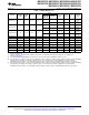
MSP430F5510, MSP430F5509, MSP430F5508, MSP430F5507 MSP430F5506, MSP430F5505, MSP430F5504, MSP430F5503 MSP430F5502, MSP430F5501, MSP430F5500 www.ti.com SLAS645I – JULY 2009 – REVISED NOVEMBER 2013 DEVICE DESCRIPTORS Table 59 list the complete contents of the device descriptor tag-length-value (TLV) structure for each device type. Table 59.
MSP430F5510, MSP430F5509, MSP430F5508, MSP430F5507 MSP430F5506, MSP430F5505, MSP430F5504, MSP430F5503 MSP430F5502, MSP430F5501, MSP430F5500 SLAS645I – JULY 2009 – REVISED NOVEMBER 2013 www.ti.com Table 59.
MSP430F5510, MSP430F5509, MSP430F5508, MSP430F5507 MSP430F5506, MSP430F5505, MSP430F5504, MSP430F5503 MSP430F5502, MSP430F5501, MSP430F5500 www.ti.com SLAS645I – JULY 2009 – REVISED NOVEMBER 2013 Table 59.
MSP430F5510, MSP430F5509, MSP430F5508, MSP430F5507 MSP430F5506, MSP430F5505, MSP430F5504, MSP430F5503 MSP430F5502, MSP430F5501, MSP430F5500 SLAS645I – JULY 2009 – REVISED NOVEMBER 2013 www.ti.com Table 60.
MSP430F5510, MSP430F5509, MSP430F5508, MSP430F5507 MSP430F5506, MSP430F5505, MSP430F5504, MSP430F5503 MSP430F5502, MSP430F5501, MSP430F5500 www.ti.com SLAS645I – JULY 2009 – REVISED NOVEMBER 2013 Table 60.
MSP430F5510, MSP430F5509, MSP430F5508, MSP430F5507 MSP430F5506, MSP430F5505, MSP430F5504, MSP430F5503 MSP430F5502, MSP430F5501, MSP430F5500 SLAS645I – JULY 2009 – REVISED NOVEMBER 2013 www.ti.com Table 60. F5500 to F5503 Device Descriptor Table(1) (continued) SIZE (bytes) F5503RGZ F5502RGZ F5501RGC F5500RGZ VALUE VALUE VALUE VALUE P1 1 50h 50h 50h 50h USCI_A1 1 92h 92h 92h 92h USCI_B1 1 93h 93h 93h 93h TA1.CCIFG0 1 66h 66h 66h 66h TA1.CCIFG1..
MSP430F5510, MSP430F5509, MSP430F5508, MSP430F5507 MSP430F5506, MSP430F5505, MSP430F5504, MSP430F5503 MSP430F5502, MSP430F5501, MSP430F5500 www.ti.
PACKAGE OPTION ADDENDUM www.ti.
PACKAGE OPTION ADDENDUM www.ti.
PACKAGE OPTION ADDENDUM www.ti.
PACKAGE OPTION ADDENDUM www.ti.com 5-Jul-2013 Pb-Free (RoHS Exempt): This component has a RoHS exemption for either 1) lead-based flip-chip solder bumps used between the die and package, or 2) lead-based die adhesive used between the die and leadframe. The component is otherwise considered Pb-Free (RoHS compatible) as defined above. Green (RoHS & no Sb/Br): TI defines "Green" to mean Pb-Free (RoHS compatible), and free of Bromine (Br) and Antimony (Sb) based flame retardants (Br or Sb do not exceed 0.
MECHANICAL DATA MTQF003A – OCTOBER 1994 – REVISED DECEMBER 1996 PT (S-PQFP-G48) PLASTIC QUAD FLATPACK 0,27 0,17 0,50 36 0,08 M 25 37 24 48 13 0,13 NOM 1 12 5,50 TYP 7,20 SQ 6,80 9,20 SQ 8,80 Gage Plane 0,25 0,05 MIN 1,45 1,35 Seating Plane 1,60 MAX 0°– 7° 0,75 0,45 0,10 4040052 / C 11/96 NOTES: A. B. C. D. All linear dimensions are in millimeters. This drawing is subject to change without notice.
IMPORTANT NOTICE Texas Instruments Incorporated and its subsidiaries (TI) reserve the right to make corrections, enhancements, improvements and other changes to its semiconductor products and services per JESD46, latest issue, and to discontinue any product or service per JESD48, latest issue. Buyers should obtain the latest relevant information before placing orders and should verify that such information is current and complete.