MSP430F673x MSP430F672x www.ti.com SLAS731C – DECEMBER 2011 – REVISED FEBRUARY 2013 MIXED SIGNAL MICROCONTROLLER FEATURES 1 • 2 • • • • • Low Supply Voltage Range: 3.6 V Down to 1.8 V Ultra-Low Power Consumption – Active Mode (AM): All System Clocks Active 265 µA/MHz at 8 MHz, 3.0 V, Flash Program Execution (Typical) 140 µA/MHz at 8 MHz, 3.
MSP430F673x MSP430F672x SLAS731C – DECEMBER 2011 – REVISED FEBRUARY 2013 www.ti.com DESCRIPTION The Texas Instruments MSP430 family of ultra-low-power microcontrollers consists of several devices featuring different sets of peripherals targeted for various applications. The architecture, combined with extensive lowpower modes, is optimized to achieve extended battery life in portable measurement applications.
MSP430F673x MSP430F672x www.ti.com SLAS731C – DECEMBER 2011 – REVISED FEBRUARY 2013 Table 2.
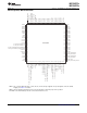
MSP430F673x MSP430F672x SLAS731C – DECEMBER 2011 – REVISED FEBRUARY 2013 www.ti.com Functional Block Diagram, MSP430F673xIPZ, MSP430F672xIPZ XIN DVCC DVSS XOUT AVCC AVSS AUX1 AUX2 AUX3 PA P1.x P2.x RST/NMI PB P3.x P4.x PC P5.x P6.x P7.x PD P8.x PE P9.
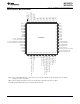
MSP430F673x MSP430F672x www.ti.com SLAS731C – DECEMBER 2011 – REVISED FEBRUARY 2013 P6.1/S18 P6.2/S17 P6.3/S16 P6.4/S15 P6.5/S14 P6.6/S13 P6.7/S12 P7.0/S11 P7.1/S10 P7.2/S9 P7.3/S8 P7.4/S7 P7.5/S6 P7.6/S5 P7.7/S4 P8.0/S3 P8.1/S2 P8.2/S1 P8.3/S0 TEST/SBWTCK PJ.0/SMCLK/TDO PJ.1/MCLK/TDI/TCLK PJ.2/ADC10CLK/TMS PJ.
MSP430F673x MSP430F672x SLAS731C – DECEMBER 2011 – REVISED FEBRUARY 2013 www.ti.com Table 3. Pinout Differences Between MSP430F673xIPZ and MSP430F672xIPZ (1) PIN NUMBER (1) 6 PIN NAME MSP430F673xIPZ MSP430F672xIPZ 1 SD0P0 SD0P0 2 SD0N0 SD0N0 3 SD1P0 SD1P0 4 SD1N0 SD1N0 5 SD2P0 NC 6 SD2N0 NC 7 VREF VREF 53 P3.4/PM_SDCLK/S39 P3.4/PM_SDCLK/S39 54 P3.5/PM_SD0DIO/S38 P3.5/PM_SD0DIO/S38 55 P3.6/PM_SD1DIO/S37 P3.6/PM_SD1DIO/S37 56 P3.7/PM_SD2DIO/S36 P3.
MSP430F673x MSP430F672x www.ti.com SLAS731C – DECEMBER 2011 – REVISED FEBRUARY 2013 P5.2/S13 P5.3/S12 P5.4/S11 P5.5/S10 P5.6/S9 P5.7/S8 P6.0/S7 P6.1/S6 P6.2/S5 P6.3/S4 P6.4/S3 P6.5/S2 P6.6/S1 P6.7/S0 TEST/SBWTCK PJ.0/SMCLK/TDO PJ.1/MCLK/TDI/TCLK PJ.2/ADC10CLK/TMS PJ.3/ACLK/TCK RST/NMI/SBWTDIO Pin Designation, MSP430F673xIPN 80 79 78 77 76 75 74 73 72 71 70 69 68 67 66 65 64 63 62 61 SD0P0 1 60 DVSS SD0N0 2 59 DVSYS SD1P0 3 58 P5.1/S14 SD1N0 4 57 P5.
MSP430F673x MSP430F672x SLAS731C – DECEMBER 2011 – REVISED FEBRUARY 2013 www.ti.com Table 4. Pinout Differences Between MSP430F673xIPN and MSP430F672xIPN (1) PIN NUMBER (1) 8 PIN NAME MSP430F673xIPN MSP430F672xIPN 1 SD0P0 SD0P0 2 SD0N0 SD0N0 3 SD1P0 SD1P0 4 SD1N0 SD1N0 5 SD2P0 NC 6 SD2N0 NC 7 VREF VREF 45 P3.4/PM_SDCLK/S27 P3.4/PM_SDCLK/S27 46 P3.5/PM_SD0DIO/S26 P3.5/PM_SD0DIO/S26 47 P3.6/PM_SD1DIO/S25 P3.6/PM_SD1DIO/S25 48 P3.7/PM_SD2DIO/S24 P3.
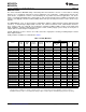
MSP430F673x MSP430F672x www.ti.com SLAS731C – DECEMBER 2011 – REVISED FEBRUARY 2013 Table 5. Terminal Functions, MSP430F67xxIPZ TERMINAL NAME NO.
MSP430F673x MSP430F672x SLAS731C – DECEMBER 2011 – REVISED FEBRUARY 2013 www.ti.com Table 5. Terminal Functions, MSP430F67xxIPZ (continued) TERMINAL NAME NO. I/O (1) DESCRIPTION PZ XOUT 25 AUXVCC3 26 Auxiliary power supply AUXVCC3 for back up subsystem P1.
MSP430F673x MSP430F672x www.ti.com SLAS731C – DECEMBER 2011 – REVISED FEBRUARY 2013 Table 5. Terminal Functions, MSP430F67xxIPZ (continued) TERMINAL NAME NO. I/O (1) DESCRIPTION PZ P2.4/PM_UCA1CLK 45 I/O General-purpose digital I/O with port interrupt and mappable secondary function Default mapping: eUSCI_A1 clock input/output P2.5/PM_UCA2CLK 46 I/O General-purpose digital I/O with port interrupt and mappable secondary function Default mapping: eUSCI_A2 clock input/output P2.6/PM_TA1.
MSP430F673x MSP430F672x SLAS731C – DECEMBER 2011 – REVISED FEBRUARY 2013 www.ti.com Table 5. Terminal Functions, MSP430F67xxIPZ (continued) TERMINAL NAME NO. I/O (1) DESCRIPTION PZ P4.6/S29 63 I/O General-purpose digital I/O LCD segment output S29 P4.7/S28 64 I/O General-purpose digital I/O LCD segment output S28 P5.0/S27 65 I/O General-purpose digital I/O LCD segment output S27 P5.1/S26 66 I/O General-purpose digital I/O LCD segment output S26 P5.
MSP430F673x MSP430F672x www.ti.com SLAS731C – DECEMBER 2011 – REVISED FEBRUARY 2013 Table 5. Terminal Functions, MSP430F67xxIPZ (continued) TERMINAL NAME NO. I/O (1) DESCRIPTION PZ P7.2/S9 85 I/O General-purpose digital I/O LCD segment output S9 P7.3/S8 86 I/O General-purpose digital I/O LCD segment output S8 P7.4/S7 87 I/O General-purpose digital I/O LCD segment output S7 P7.5/S6 88 I/O General-purpose digital I/O LCD segment output S6 P7.
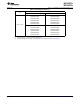
MSP430F673x MSP430F672x SLAS731C – DECEMBER 2011 – REVISED FEBRUARY 2013 www.ti.com Table 6. Terminal Functions, MSP430F67xxIPN TERMINAL NAME NO.
MSP430F673x MSP430F672x www.ti.com SLAS731C – DECEMBER 2011 – REVISED FEBRUARY 2013 Table 6. Terminal Functions, MSP430F67xxIPN (continued) TERMINAL NAME NO. I/O (1) DESCRIPTION PN P1.
MSP430F673x MSP430F672x SLAS731C – DECEMBER 2011 – REVISED FEBRUARY 2013 www.ti.com Table 6. Terminal Functions, MSP430F67xxIPN (continued) TERMINAL NAME P3.0/PM_TA2.0/S31/BSL_TX P3.1/PM_TA2.1/S30/BSL_RX NO.
MSP430F673x MSP430F672x www.ti.com SLAS731C – DECEMBER 2011 – REVISED FEBRUARY 2013 Table 6. Terminal Functions, MSP430F67xxIPN (continued) TERMINAL NAME NO. I/O (1) DESCRIPTION PN P5.0/S15 57 I/O General-purpose digital I/O LCD segment output S15 P5.1/S14 58 I/O General-purpose digital I/O LCD segment output S14 DVSYS (5) 59 Digital power supply for I/Os DVSS 60 Digital ground supply P5.2/S13 61 I/O General-purpose digital I/O LCD segment output S13 P5.
MSP430F673x MSP430F672x SLAS731C – DECEMBER 2011 – REVISED FEBRUARY 2013 www.ti.com Table 6. Terminal Functions, MSP430F67xxIPN (continued) TERMINAL NAME NO. I/O (1) DESCRIPTION PN PJ.2/ADC10CLK/TMS 78 I/O General-purpose digital I/O ADC10_A clock output Test mode select PJ.
MSP430F673x MSP430F672x www.ti.com SLAS731C – DECEMBER 2011 – REVISED FEBRUARY 2013 SHORT-FORM DESCRIPTION CPU The MSP430 CPU has a 16-bit RISC architecture that is highly transparent to the application. All operations, other than program-flow instructions, are performed as register operations in conjunction with seven addressing modes for source operand and four addressing modes for destination operand.
MSP430F673x MSP430F672x SLAS731C – DECEMBER 2011 – REVISED FEBRUARY 2013 www.ti.com Operating Modes The MSP430 has one active mode and seven software selectable low-power modes of operation. An interrupt event can wake up the device from any of the low-power modes, service the request, and restore back to the low-power mode on return from the interrupt program.
MSP430F673x MSP430F672x www.ti.com SLAS731C – DECEMBER 2011 – REVISED FEBRUARY 2013 Interrupt Vector Addresses The interrupt vectors and the power-up start address are located in the address range 0FFFFh to 0FF80h. The vector contains the 16-bit address of the appropriate interrupt-handler instruction sequence. Table 9.
MSP430F673x MSP430F672x SLAS731C – DECEMBER 2011 – REVISED FEBRUARY 2013 www.ti.com Table 9. Interrupt Sources, Flags, and Vectors of MSP430F67xx Configurations (continued) (5) INTERRUPT SOURCE INTERRUPT FLAG Reserved Reserved (5) SYSTEM INTERRUPT WORD ADDRESS PRIORITY 0FFCEh 39 ⋮ ⋮ 0FF80h 0, lowest Reserved interrupt vectors at addresses are not used in this device and can be used for regular program code if necessary.
MSP430F673x MSP430F672x www.ti.
MSP430F673x MSP430F672x SLAS731C – DECEMBER 2011 – REVISED FEBRUARY 2013 www.ti.com Bootstrap Loader (BSL) The BSL enables users to program the flash memory or RAM using various serial interfaces. Access to the device memory via the BSL is protected by an user-defined password. BSL entry requires a specific entry sequence on the RST/NMI/SBWTDIO and TEST/SBWTCK pins. For complete description of the features of the BSL and its implementation, see MSP430 Programming via the Bootstrap Loader (BSL) (SLAU319).
MSP430F673x MSP430F672x www.ti.com SLAS731C – DECEMBER 2011 – REVISED FEBRUARY 2013 Flash Memory The flash memory can be programmed via the JTAG port, Spy-Bi-Wire (SBW), the BSL, or in-system by the CPU. The CPU can perform single-byte, single-word, and long-word writes to the flash memory. Features of the flash memory include: • Flash memory has n segments of main memory and four segments of information memory (A to D) of 128 bytes each. Each segment in main memory is 512 bytes in size.
MSP430F673x MSP430F672x SLAS731C – DECEMBER 2011 – REVISED FEBRUARY 2013 www.ti.com Power Management Module (PMM) The PMM includes an integrated voltage regulator that supplies the core voltage to the device and contains programmable output levels to provide for power optimization. The PMM also includes supply voltage supervisor (SVS) and supply voltage monitoring (SVM) circuitry, as well as brownout protection.
MSP430F673x MSP430F672x www.ti.com SLAS731C – DECEMBER 2011 – REVISED FEBRUARY 2013 Port Mapping Controller The port mapping controller allows flexible and reconfigurable mapping of digital functions to P1, P2, and P3. Table 14.
MSP430F673x MSP430F672x SLAS731C – DECEMBER 2011 – REVISED FEBRUARY 2013 www.ti.com Table 15. Default Mapping PIN NAME PZ PN PxMAPy MNEMONIC INPUT PIN FUNCTION OUTPUT PIN FUNCTION P1.0/PM_TA0.0/ VeREF-/A2 P1.0/PM_TA0.0/ VeREF-/A2 PM_TA0.0 TA0 CCR0 capture input CCI0A TA0 CCR0 compare output Out0 P1.1/PM_TA0.1/ VeREF+/A1 P1.1/PM_TA0.1/ VeREF+/A1 PM_TA0.1 TA0 CCR1 capture input CCI1A TA0 CCR1 compare output Out1 P1.2/PM_UCA0RXD/ PM_UCA0SOMI/A0 P1.
MSP430F673x MSP430F672x www.ti.com SLAS731C – DECEMBER 2011 – REVISED FEBRUARY 2013 System Module (SYS) The SYS module handles many of the system functions within the device. These include power on reset (POR) and power up clear (PUC) handling, NMI source selection and management, reset interrupt vector generators, boot strap loader entry mechanisms, as well as, configuration management (device descriptors).
MSP430F673x MSP430F672x SLAS731C – DECEMBER 2011 – REVISED FEBRUARY 2013 www.ti.com DMA Controller The DMA controller allows movement of data from one memory address to another without CPU intervention. For example, the DMA controller can be used to move data from the ADC10_A conversion memory to RAM. Using the DMA controller can increase the throughput of peripheral modules.
MSP430F673x MSP430F672x www.ti.com SLAS731C – DECEMBER 2011 – REVISED FEBRUARY 2013 CRC16 The CRC16 module produces a signature based on a sequence of entered data values and can be used for data checking purposes. The CRC16 module signature is based on the CRC-CCITT standard. Hardware Multiplier The multiplication operation is supported by a dedicated peripheral module. The module performs operations with 32-bit, 24-bit, 16-bit, and 8-bit operands.
MSP430F673x MSP430F672x SLAS731C – DECEMBER 2011 – REVISED FEBRUARY 2013 www.ti.com TA0 TA0 is a 16-bit timer/counter (Timer_A type) with three capture/compare registers. TA0 can support multiple capture/compares, PWM outputs, and interval timing. TA0 also has extensive interrupt capabilities. Interrupts may be generated from the counter on overflow conditions and from each of the capture/compare registers. Table 18.
MSP430F673x MSP430F672x www.ti.com SLAS731C – DECEMBER 2011 – REVISED FEBRUARY 2013 TA2 TA2 is a 16-bit timer/counter (Timer_A type) with two capture/compare registers. TA2 can support multiple capture/compares, PWM outputs, and interval timing. TA2 also has extensive interrupt capabilities. Interrupts may be generated from the counter on overflow conditions and from each of the capture/compare registers. Table 20.
MSP430F673x MSP430F672x SLAS731C – DECEMBER 2011 – REVISED FEBRUARY 2013 www.ti.com SD24_B Triggers Table 22 shows the input trigger connections to SD24_B converters from Timer_A modules and output trigger pulse connection from SD24_B to ADC10_A. Table 22. SD24_B Input/Output Trigger Connections DEVICE INPUT SIGNAL MODULE INPUT SIGNAL TA0.1 (internal) SD24_B SD24SCSx = {1} TA2.1 (internal) SD24_B SD24SCSx = {2} TA3.
MSP430F673x MSP430F672x www.ti.com SLAS731C – DECEMBER 2011 – REVISED FEBRUARY 2013 Peripheral File Map Table 24.
MSP430F673x MSP430F672x SLAS731C – DECEMBER 2011 – REVISED FEBRUARY 2013 www.ti.com Table 25. Special Function Registers (Base Address: 0100h) REGISTER DESCRIPTION REGISTER OFFSET SFR interrupt enable SFRIE1 00h SFR interrupt flag SFRIFG1 02h SFR reset pin control SFRRPCR 04h Table 26.
MSP430F673x MSP430F672x www.ti.com SLAS731C – DECEMBER 2011 – REVISED FEBRUARY 2013 Table 32.
MSP430F673x MSP430F672x SLAS731C – DECEMBER 2011 – REVISED FEBRUARY 2013 www.ti.com Table 37. Port Mapping for Port P3 (Base Address: 01D8h) REGISTER DESCRIPTION REGISTER OFFSET Port P3.0 mapping register P3MAP0 00h Port P3.1 mapping register P3MAP3 01h Port P3.2 mapping register P3MAP2 02h Port P3.3 mapping register P3MAP3 03h Port P3.4 mapping register P3MAP4 04h Port P3.5 mapping register P3MAP5 05h Port P3.6 mapping register P3MAP6 06h Port P3.
MSP430F673x MSP430F672x www.ti.com SLAS731C – DECEMBER 2011 – REVISED FEBRUARY 2013 Table 40.
MSP430F673x MSP430F672x SLAS731C – DECEMBER 2011 – REVISED FEBRUARY 2013 www.ti.com Table 44.
MSP430F673x MSP430F672x www.ti.com SLAS731C – DECEMBER 2011 – REVISED FEBRUARY 2013 Table 48. Backup Memory Registers (Base Address: 0480h) REGISTER DESCRIPTION REGISTER OFFSET Backup Memory 0 BAKMEM0 00h Backup Memory 1 BAKMEM1 02h Backup Memory 2 BAKMEM2 04h Backup Memory 3 BAKMEM3 06h Table 49.
MSP430F673x MSP430F672x SLAS731C – DECEMBER 2011 – REVISED FEBRUARY 2013 www.ti.com Table 50.
MSP430F673x MSP430F672x www.ti.com SLAS731C – DECEMBER 2011 – REVISED FEBRUARY 2013 Table 53. DMA Channel 1 Registers (Base Address: 0500h) REGISTER DESCRIPTION REGISTER OFFSET DMA channel 1 control DMA1CTL 20h DMA channel 1 source address low DMA1SAL 22h DMA channel 1 source address high DMA1SAH 24h DMA channel 1 destination address low DMA1DAL 26h DMA channel 1 destination address high DMA1DAH 28h DMA channel 1 transfer size DMA1SZ 2Ah Table 54.
MSP430F673x MSP430F672x SLAS731C – DECEMBER 2011 – REVISED FEBRUARY 2013 www.ti.com Table 56. eUSCI_A1 Registers (Base Address:05E0h) (continued) REGISTER DESCRIPTION REGISTER OFFSET eUSCI_A interrupt flags UCA1IFG 1Ch eUSCI_A interrupt vector word UCA1IV 1Eh Table 57.
MSP430F673x MSP430F672x www.ti.com SLAS731C – DECEMBER 2011 – REVISED FEBRUARY 2013 Table 59.
MSP430F673x MSP430F672x SLAS731C – DECEMBER 2011 – REVISED FEBRUARY 2013 www.ti.com Table 61.
MSP430F673x MSP430F672x www.ti.com SLAS731C – DECEMBER 2011 – REVISED FEBRUARY 2013 Absolute Maximum Ratings (1) over operating free-air temperature range (unless otherwise noted) Voltage applied at DVCC to DVSS Voltage applied to any pin (excluding VCORE) -0.3 V to 4.1 V (2) -0.3 V to VCC + 0.
MSP430F673x MSP430F672x SLAS731C – DECEMBER 2011 – REVISED FEBRUARY 2013 www.ti.com 25 System Frequency - MHz 3 20 2 2, 3 1 1, 2 1, 2, 3 0, 1 0, 1, 2 0, 1, 2, 3 12 8 0 0 1.8 2.0 2.2 2.4 3.6 Supply Voltage - V The numbers within the fields denote the supported PMMCOREVx settings. Figure 1.
MSP430F673x MSP430F672x www.ti.
MSP430F673x MSP430F672x SLAS731C – DECEMBER 2011 – REVISED FEBRUARY 2013 www.ti.com Low-Power Mode With LCD Supply Currents (Into VCC) Excluding External Current over recommended ranges of supply voltage and operating free-air temperature (unless otherwise noted) (1) (2) Temperature (TA) PARAMETER VCC PMMCOREVx -40°C TYP ILPM3 LCD, int. bias Low-power mode 3 (LPM3) current, LCD 4mux mode, internal biasing, charge pump disabled (3) (4) ILPM3 LCD, int.
MSP430F673x MSP430F672x www.ti.com SLAS731C – DECEMBER 2011 – REVISED FEBRUARY 2013 Inputs – Ports P1 and P2 (1) over recommended ranges of supply voltage and operating free-air temperature (unless otherwise noted) t(int) (1) (2) PARAMETER TEST CONDITIONS VCC External interrupt timing (2) Port P1, P2: P1.x to P2.x, External trigger pulse width to set interrupt flag 2.2 V/3 V MIN MAX 20 UNIT ns Some devices may contain additional ports with interrupts.
MSP430F673x MSP430F672x SLAS731C – DECEMBER 2011 – REVISED FEBRUARY 2013 www.ti.com Typical Characteristics – General Purpose I/O (Full Drive Strength) HIGH-LEVEL OUTPUT CURRENT vs HIGH-LEVEL OUTPUT VOLTAGE HIGH-LEVEL OUTPUT CURRENT vs HIGH-LEVEL OUTPUT VOLTAGE 0 0 VCC = 3 V Full Drive Strength -10 -5 IOH – High-Level Output Current – mA IOH – High-Level Output Current – mA VCC = 1.8 V Full Drive Strength -10 -15 TA = 85°C -20 -20 -30 -40 TA = 85°C -50 TA = 25°C TA = 25°C -25 -60 0 0.
MSP430F673x MSP430F672x www.ti.com SLAS731C – DECEMBER 2011 – REVISED FEBRUARY 2013 Outputs – General Purpose I/O (Reduced Drive Strength) over recommended ranges of supply voltage and operating free-air temperature (unless otherwise noted) (1) PARAMETER TEST CONDITIONS I(OHmax) = –1 mA VOH High-level output voltage I(OHmax) = –3 mA (2) I(OHmax) = –2 mA (2) I(OHmax) = –6 mA (2) I(OLmax) = 1 mA VOL Low-level output voltage (3) (4) 1.8 V 3.
MSP430F673x MSP430F672x SLAS731C – DECEMBER 2011 – REVISED FEBRUARY 2013 www.ti.com Typical Characteristics – General Purpose I/O (Reduced Drive Strength) HIGH-LEVEL OUTPUT CURRENT vs HIGH-LEVEL OUTPUT VOLTAGE HIGH-LEVEL OUTPUT CURRENT vs HIGH-LEVEL OUTPUT VOLTAGE 0 0 VCC = 1.
MSP430F673x MSP430F672x www.ti.com SLAS731C – DECEMBER 2011 – REVISED FEBRUARY 2013 Output Frequency – General Purpose I/O over recommended ranges of supply voltage and operating free-air temperature (unless otherwise noted) PARAMETER fPx.y fPort_CLK (1) (2) TEST CONDITIONS Port output frequency (with load) See Clock output frequency ACLK SMCLK MCLK CL = 20 pF (2) (1) (2) MIN MAX VCC = 1.8 V PMMCOREVx = 0 16 VCC = 3 V PMMCOREVx = 3 25 VCC = 1.
MSP430F673x MSP430F672x SLAS731C – DECEMBER 2011 – REVISED FEBRUARY 2013 www.ti.
MSP430F673x MSP430F672x www.ti.com SLAS731C – DECEMBER 2011 – REVISED FEBRUARY 2013 DCO Frequency over recommended ranges of supply voltage and operating free-air temperature (unless otherwise noted) PARAMETER TEST CONDITIONS (1) MIN TYP MAX UNIT fDCO(0,0) DCO frequency (0, 0) DCORSELx = 0, DCOx = 0, MODx = 0 0.07 0.20 MHz fDCO(0,31) DCO frequency (0, 31) (1) DCORSELx = 0, DCOx = 31, MODx = 0 0.70 1.70 MHz fDCO(1,0) DCO frequency (1, 0) (1) DCORSELx = 1, DCOx = 0, MODx = 0 0.15 0.
MSP430F673x MSP430F672x SLAS731C – DECEMBER 2011 – REVISED FEBRUARY 2013 www.ti.com PMM, Brown-Out Reset (BOR) over recommended ranges of supply voltage and operating free-air temperature (unless otherwise noted) PARAMETER TEST CONDITIONS V(DVCC_BOR_IT–) BORH on voltage, DVCC falling level | dDVCC/dt | < 3 V/s V(DVCC_BOR_IT+) BORH off voltage, DVCC rising level | dDVCC/dt | < 3 V/s V(DVCC_BOR_hys) BORH hysteresis tRESET (1) (1) MIN TYP 0.80 1.
MSP430F673x MSP430F672x www.ti.com SLAS731C – DECEMBER 2011 – REVISED FEBRUARY 2013 PMM, SVM High Side over recommended ranges of supply voltage and operating free-air temperature (unless otherwise noted) PARAMETER TEST CONDITIONS MIN SVMHE = 0, DVCC = 3.6 V I(SVMH) V(SVMH) SVMH current consumption SVMH on/off voltage level (1) t(SVMH) (1) SVMH propagation delay SVMH on/off delay time MAX UNIT 0 nA SVMHE = 1, DVCC = 3.6 V, SVMHFP = 0 200 nA SVMHE = 1, DVCC = 3.6 V, SVMHFP = 1 1.
MSP430F673x MSP430F672x SLAS731C – DECEMBER 2011 – REVISED FEBRUARY 2013 www.ti.com PMM, SVS Low Side over recommended ranges of supply voltage and operating free-air temperature (unless otherwise noted) PARAMETER TEST CONDITIONS MIN TYP SVSLE = 0, PMMCOREV = 2 I(SVSL) SVSL current consumption tpd(SVSL) t(SVSL) SVSL propagation delay SVSL on/off delay time MAX UNIT 0 nA SVSLE = 1, PMMCOREV = 2, SVSLFP = 0 200 nA SVSLE = 1, PMMCOREV = 2, SVSLFP = 1 1.
MSP430F673x MSP430F672x www.ti.com SLAS731C – DECEMBER 2011 – REVISED FEBRUARY 2013 Auxiliary Supplies - Recommended Operating Conditions over operating free-air temperature range (unless otherwise noted) MIN VCC NOM MAX Supply voltage range for all supplies at pins DVCC, AVCC, AUX1, AUX2, AUX3 1.8 3.6 PMMCOREVx = 0 1.8 3.6 PMMCOREVx = 1 2.0 3.6 PMMCOREVx = 2 2.2 3.6 2.4 3.
MSP430F673x MSP430F672x SLAS731C – DECEMBER 2011 – REVISED FEBRUARY 2013 www.ti.com 0.7 0.6 ICC, monitor – µA 0.5 0.4 0.3 0.2 0.1 0 1.8 2 2.2 2.4 2.6 2.8 VDSYS Voltage – V 3 3.2 3.4 3.6 3.2 3.4 3.6 Figure 11. VDSYS Voltage vs ICC,Monitor 120 Imeas, monitor – nA 100 80 60 40 20 0 1.8 2.0 2.2 2.4 2.6 2.8 AUXVCC1 Voltage – V 3.0 Figure 12.
MSP430F673x MSP430F672x www.ti.com SLAS731C – DECEMBER 2011 – REVISED FEBRUARY 2013 Auxiliary Supplies - Switching Time over operating free-air temperature range (unless otherwise noted) PARAMETER TEST CONDITIONS tSwitch Time from occurence of trigger (SVM or software) to "new" supply connected to system supplies tRecover "Recovery time" after a switch over took place. During that time no further switching takes place.
MSP430F673x MSP430F672x SLAS731C – DECEMBER 2011 – REVISED FEBRUARY 2013 www.ti.com Timer_A over recommended ranges of supply voltage and operating free-air temperature (unless otherwise noted) PARAMETER TEST CONDITIONS VCC fTA Timer_A input clock frequency Internal: SMCLK, ACLK External: TACLK Duty cycle = 50% ± 10% 1.8 V/ 3.0 V tTA,cap Timer_A capture timing All capture inputs. Minimum pulse width required for capture. 1.8 V/ 3.
MSP430F673x MSP430F672x www.ti.com SLAS731C – DECEMBER 2011 – REVISED FEBRUARY 2013 eUSCI (SPI Master Mode) (continued) over recommended ranges of supply voltage and operating free-air temperature (unless otherwise noted)(1) PARAMETER TEST CONDITIONS VCC tHD,MI SOMI input data hold time tVALID,MO SIMO output data valid time (2) UCLK edge to SIMO valid, CL = 20 pF tHD,MO SIMO output data hold time (3) CL = 20 pF (2) (3) MIN 2.0 V 0 3.0 V 0 TYP MAX ns 2.0 V 9 3.0 V 5 2.0 V 0 3.
MSP430F673x MSP430F672x SLAS731C – DECEMBER 2011 – REVISED FEBRUARY 2013 www.ti.com UCMODEx = 01 tSTE,LEAD STE tSTE,LAG UCMODEx = 10 1/fUCxCLK CKPL = 0 UCLK CKPL = 1 tLOW/HIGH tLOW/HIGH tHD,MI tSU,MI SOMI tSTE,ACC tSTE,DIS tVALID,MO SIMO Figure 14.
MSP430F673x MSP430F672x www.ti.
MSP430F673x MSP430F672x SLAS731C – DECEMBER 2011 – REVISED FEBRUARY 2013 www.ti.com UCMODEx = 01 tSTE,LEAD STE tSTE,LAG UCMODEx = 10 1/fUCxCLK CKPL = 0 UCLK CKPL = 1 tLOW/HIGH tLOW/HIGH tHD,SI tSU,SI SIMO tACC tDIS tVALID,SO SOMI Figure 16.
MSP430F673x MSP430F672x www.ti.
MSP430F673x MSP430F672x SLAS731C – DECEMBER 2011 – REVISED FEBRUARY 2013 www.ti.
MSP430F673x MSP430F672x www.ti.com SLAS731C – DECEMBER 2011 – REVISED FEBRUARY 2013 SD24_B, Power Supply and Recommended Operating Conditions MIN AVCC Analog supply voltage fSD AVCC = DVCC, AVSS = DVSS = 0 V TYP MAX UNIT 2.4 3.6 V Modulator clock frequency (1) 0.03 2.
MSP430F673x MSP430F672x SLAS731C – DECEMBER 2011 – REVISED FEBRUARY 2013 www.ti.com 1600 Input Leakage Current – nA 1400 1200 1000 800 600 400 200 0 -200 -1 -0.5 0 0.5 1 Input Voltage – V 1.5 2 2.5 3 Figure 18.
MSP430F673x MSP430F672x www.ti.
MSP430F673x MSP430F672x SLAS731C – DECEMBER 2011 – REVISED FEBRUARY 2013 www.ti.
MSP430F673x MSP430F672x www.ti.
MSP430F673x MSP430F672x SLAS731C – DECEMBER 2011 – REVISED FEBRUARY 2013 www.ti.
MSP430F673x MSP430F672x www.ti.com SLAS731C – DECEMBER 2011 – REVISED FEBRUARY 2013 90 85 SINAD – dB 80 75 70 65 60 0.1 0.2 0.3 0.4 0.5 0.6 Vpp/Vref/Gain 0.7 0.8 0.9 1 Figure 20. SINAD vs VPP SD24_B, External Reference Input ensure correct input voltage range according to VREF VCC MIN TYP MAX VREF(I) Input voltage PARAMETER SD24REFS = 0 TEST CONDITIONS 3V 1.0 1.20 1.
MSP430F673x MSP430F672x SLAS731C – DECEMBER 2011 – REVISED FEBRUARY 2013 www.ti.com 10-Bit ADC, Timing Parameters over recommended ranges of supply voltage and operating free-air temperature (unless otherwise noted) PARAMETER VCC MIN TYP MAX UNIT For specified performance of ADC10_A linearity parameters 2.2 V, 3 V 0.45 5 5.5 MHz Internal ADC10_A oscillator (1) ADC10DIV = 0, fADC10CLK = fADC10OSC 2.2 V, 3 V 4.4 5.0 5.6 MHz 2.2 V, 3 V 2.
MSP430F673x MSP430F672x www.ti.com SLAS731C – DECEMBER 2011 – REVISED FEBRUARY 2013 10-Bit ADC, Linearity Parameters over recommended ranges of supply voltage and operating free-air temperature (unless otherwise noted) PARAMETER TEST CONDITIONS VCC MIN TYP MAX UNIT EI Integral linearity error 1.4 V ≤ (VeREF+ – VeREF–)min ≤ 1.6 V ED Differential linearity error (VeREF+ – VeREF–)min ≤ (VeREF+ – VeREF–), CVeREF+ = 20 pF 2.2 V, 3 V ±1.
MSP430F673x MSP430F672x SLAS731C – DECEMBER 2011 – REVISED FEBRUARY 2013 www.ti.com REF, Built-In Reference over recommended ranges of supply voltage and operating free-air temperature (unless otherwise noted) PARAMETER Positive built-in reference voltage VREF+ AVCC(min) AVCC minimum voltage, Positive built-in reference active Operating supply current into AVCC terminal (1) IREF+ TEST CONDITIONS VCC MIN TYP MAX REFVSEL = {2} for 2.5 V, REFON = 1 3V 2.47 2.51 2.55 REFVSEL = {1} for 2.
MSP430F673x MSP430F672x www.ti.com SLAS731C – DECEMBER 2011 – REVISED FEBRUARY 2013 Flash Memory over recommended ranges of supply voltage and operating free-air temperature (unless otherwise noted) PARAMETER TEST CONDITIONS DVCC(PGM/ERASE) Program and erase supply voltage MIN TYP 1.8 MAX 3.
MSP430F673x MSP430F672x SLAS731C – DECEMBER 2011 – REVISED FEBRUARY 2013 www.ti.com INPUT/OUTPUT SCHEMATICS Port P1, P1.0 and P1.1, Input/Output With Schmitt Trigger (MSP430F67xxIPZ and MSP430F67xxIPN) Pad Logic to/from Reference To ADC10_A INCHx = y P1REN.x P1MAP.x = PMAP_ANALOG P1DIR.x 0 from Port Mapping 1 P1OUT.x 0 from Port Mapping 1 DVSS 0 DVCC 1 1 Direction 0: Input 1: Output P1.0/PM_TA0.0/VeREF-/A2 P1.1/PM_TA0.1/VeREF+/A1 P1DS.x 0: Low drive 1: High drive P1SEL.x P1IN.
MSP430F673x MSP430F672x www.ti.com SLAS731C – DECEMBER 2011 – REVISED FEBRUARY 2013 Port P1, P1.2, Input/Output With Schmitt Trigger (MSP430F67xxIPZ and MSP430F67xxIPN) Pad Logic To ADC10_A INCHx = y P1REN.x P1MAP.x = PMAP_ANALOG P1DIR.x 0 from Port Mapping 1 P1OUT.x 0 from Port Mapping 1 DVSS 0 DVCC 1 1 Direction 0: Input 1: Output P1.2/PM_UCA0RXD/PM_UCA0SOMI/A0 P1DS.x 0: Low drive 1: High drive P1SEL.x P1IN.x Bus Keeper EN to Port Mapping D P1IE.x EN P1IRQ.x Q P1IFG.x P1SEL.
MSP430F673x MSP430F672x SLAS731C – DECEMBER 2011 – REVISED FEBRUARY 2013 www.ti.com Port P1, P1.3 to P1.5, Input/Output With Schmitt Trigger (MSP430F67xxIPZ and MSP430F67xxIPN) to LCD_C Pad Logic P1REN.x P1MAP.x = PMAP_ANALOG P1DIR.x 0 from Port Mapping 1 P1OUT.x 0 from Port Mapping 1 DVSS 0 DVCC 1 1 Direction 0: Input 1: Output P1DS.x 0: Low drive 1: High drive P1SEL.x P1.3/PM_UCA0TXD/PM_UCA0SIMO/R03 P1.4/PM_UCA1RXD/PM_UCA1SOMI/LCDREF/R13 P1.5/PM_UCA1TXD/PM_UCA1SIMO/R23 P1IN.
MSP430F673x MSP430F672x www.ti.com SLAS731C – DECEMBER 2011 – REVISED FEBRUARY 2013 Port P1, P1.6 and P1.7 (MSP430F67xxIPZ and MSP430F67xxIPN), Port P2, P2.0 and P2.1 (MSP430F67xxIPZ Only) Input/Output With Schmitt Trigger COM4 to COM7 from LCD_C Pad Logic PyREN.x PyMAP.x = PMAP_ANALOG PyDIR.x 0 from Port Mapping 1 PyOUT.x 0 from Port Mapping 1 DVSS 0 DVCC 1 1 Direction 0: Input 1: Output PyDS.x 0: Low drive 1: High drive PySEL.x P1.6/PM_UCA0CLK/COM4 P1.7/PM_UCB0CLK/COM5 P2.
MSP430F673x MSP430F672x SLAS731C – DECEMBER 2011 – REVISED FEBRUARY 2013 www.ti.com Table 66. Port P1 (P1.6 and P1.7) Pin Functions (MSP430F67xxIPZ and MSP430F67xxIPN) CONTROL BITS/SIGNALS (1) PIN NAME (P1.x) P1.6/PM_UCA0CLK/COM4 x 6 FUNCTION (1) 7 COM4,5 Enable Signal 0 X 0 1 default 0 X 1 = 31 0 P1SEL.x P1.6 (I/O) I: 0; O: 1 UCA0CLK X Output driver and input Schmitt trigger disabled COM4 P1.7/PM_UCB0CLK/COM5 P1MAPx P1DIR.x X X X 1 P1.
MSP430F673x MSP430F672x www.ti.com SLAS731C – DECEMBER 2011 – REVISED FEBRUARY 2013 Port P2, P2.2 to P2.7, Input/Output With Schmitt Trigger (MSP430F67xxIPZ Only) Pad Logic P2REN.x P2MAP.x = PMAP_ANALOG P2DIR.x 0 from Port Mapping 1 P2OUT.x 0 from Port Mapping 1 DVSS 0 DVCC 1 Direction 0: Input 1: Output P2DS.x 0: Low drive 1: High drive P2SEL.x P2IN.x P2.2/PM_UCA2RXD/PM_UCA2SOMI P2.3/PM_UCA2TXD/PM_UCA2SIMO P2.4/PM_UCA1CLK P2.5/PM_UCA2CLK P2.6/PM_TA1.0 P2.7/PM_TA1.
MSP430F673x MSP430F672x SLAS731C – DECEMBER 2011 – REVISED FEBRUARY 2013 www.ti.com Table 68. Port P2 (P2.2 to P2.7) Pin Functions (MSP430F67xxIPZ Only) PIN NAME (P2.x) x P2.2/PM_UCA2RXD/ PM_UCA2SOMI 2 P2.3/PM_UCA2TXD/ PM_UCA2SIMO 3 FUNCTION P2.2 (I/O) UCA2RXD/UCA2SOMI Output driver and input Schmitt trigger disabled P2.4/PM_UCA1CLK P2.5/PM_UCA2CLK P2.6/PM_TA1.0 4 5 6 (1) 88 7 P2DIR.x P2SEL.
MSP430F673x MSP430F672x www.ti.com SLAS731C – DECEMBER 2011 – REVISED FEBRUARY 2013 Port P3, P3.0 to P3.3, Input/Output With Schmitt Trigger (MSP430F67xxIPZ Only) Pad Logic P3REN.x P3MAP.x = PMAP_ANALOG P3DIR.x 0 from Port Mapping 1 P3OUT.x 0 from Port Mapping 1 DVSS 0 DVCC 1 1 Direction 0: Input 1: Output P3.0/PM_TA2.0 P3.1/PM_TA2.1 P3.2/PM_TACLK/PM_RTCCLK P3.3/PM_TA0.2 P3DS.x 0: Low drive 1: High drive P3SEL.x P3IN.x Bus Keeper EN to Port Mapping D Table 69. Port P3 (P3.0 to P3.
MSP430F673x MSP430F672x SLAS731C – DECEMBER 2011 – REVISED FEBRUARY 2013 www.ti.com Port P3, P3.4 to P3.7 , Input/Output With Schmitt Trigger (MSP430F67xxIPZ Only) S39 to S37 LCDS39 to LCDS37 Pad Logic P3REN.x P3MAP.x = PMAP_ANALOG P3DIR.x 0 from Port Mapping 1 P3OUT.x 0 from Port Mapping 1 DVSS 0 DVCC 1 1 Direction 0: Input 1: Output P3.4/PM_SDCLK/S39 P3.5/PM_SD0DIO/S38 P3.6/PM_SD1DIO/S37 P3.7/PM_SD2DIO/S36 P3DS.x 0: Low drive 1: High drive P3SEL.x P3IN.
MSP430F673x MSP430F672x www.ti.com SLAS731C – DECEMBER 2011 – REVISED FEBRUARY 2013 Port P4, Port P5, Port P6, Port P7, Port P8, P8.0 to P8.3 Input/Output With Schmitt Trigger (MSP430F67xxIPZ Only) Sz LCDSz Pad Logic PyREN.x PyDIR.x 0 0 DVSS 1 0 DVCC 1 1 Direction 0: Input 1: Output 1 PyOUT.x DVSS PyDS.x 0: Low drive 1: High drive PySEL.x Py.x/Sz PyIN.
MSP430F673x MSP430F672x SLAS731C – DECEMBER 2011 – REVISED FEBRUARY 2013 www.ti.com Table 71. Port P4 (P4.0 to P4.7) Pin Functions (MSP430F67xxIPZ Only) PIN NAME (P4.x) P4.0/S35 P4.1/S34 x 0 1 FUNCTION P4.0 (I/O) 2 3 P4.5/S30 P4.6/S29 4 5 6 0 0 1 0 DVSS 1 1 0 S35 X X 1 P4.1 (I/O) I: 0; O: 1 0 0 N/A 0 1 0 DVSS 1 1 0 P4.2 (I/O) 7 92 X 1 0 0 0 1 0 1 1 0 S33 X X 1 I: 0; O: 1 0 0 0 1 0 P4.
MSP430F673x MSP430F672x www.ti.com SLAS731C – DECEMBER 2011 – REVISED FEBRUARY 2013 Table 72. Port P5 (P5.0 to P5.7) Pin Functions (MSP430F67xxIPZ Only) PIN NAME (P5.x) P5.0/S27 P5.1/S26 x 0 1 FUNCTION P5.0 (I/O) 2 3 P5.5/S22 P5.6/S21 4 5 6 0 0 1 0 DVSS 1 1 0 S27 X X 1 P5.1 (I/O) I: 0; O: 1 0 0 N/A 0 1 0 DVSS 1 1 0 P5.2 (I/O) 7 X 1 0 0 0 1 0 1 1 0 S25 X X 1 I: 0; O: 1 0 0 0 1 0 P5.
MSP430F673x MSP430F672x SLAS731C – DECEMBER 2011 – REVISED FEBRUARY 2013 www.ti.com Table 73. Port P6 (P6.0 to P6.7) Pin Functions (MSP430F67xxIPZ Only) PIN NAME (P6.x) P6.0/S19 P6.1/S18 x 0 1 FUNCTION P6.0 (I/O) 2 3 P6.5/S14 P6.6/S13 4 5 6 0 0 1 0 DVSS 1 1 0 S19 X X 1 P6.1 (I/O) I: 0; O: 1 0 0 N/A 0 1 0 DVSS 1 1 0 P6.2 (I/O) 7 94 X 1 0 0 0 1 0 1 1 0 S17 X X 1 I: 0; O: 1 0 0 0 1 0 P6.
MSP430F673x MSP430F672x www.ti.com SLAS731C – DECEMBER 2011 – REVISED FEBRUARY 2013 Table 74. Port P7 (P7.0 to P7.7) Pin Functions (MSP430F67xxIPZ Only) PIN NAME (P7.x) P7.0/S11 P7.1/S10 x 0 1 FUNCTION P7.0 (I/O) 2 3 P7.5/S6 P7.6/S5 4 5 6 0 0 1 0 DVSS 1 1 0 S11 X X 1 P7.1 (I/O) I: 0; O: 1 0 0 N/A 0 1 0 DVSS 1 1 0 P7.2 (I/O) 7 X 1 0 0 0 1 0 1 1 0 S9 X X 1 I: 0; O: 1 0 0 0 1 0 P7.
MSP430F673x MSP430F672x SLAS731C – DECEMBER 2011 – REVISED FEBRUARY 2013 www.ti.com Table 75. Port P8 (P8.0 to P8.3) Pin Functions (MSP430F67xxIPZ Only) PIN NAME (P8.x) P8.0/S3 P8.1/S2 x 0 1 FUNCTION P8.0 (I/O) 2 3 96 LCDS3...0 0 0 0 1 0 DVSS 1 1 0 S3 X X 1 P8.1 (I/O) I: 0; O: 1 0 0 N/A 0 1 0 DVSS 1 1 0 P8.2 (I/O) X X 1 I: 0; O: 1 0 0 0 1 0 DVSS 1 1 0 S1 X X 1 I: 0; O: 1 0 0 0 1 0 P8.3 (I/O) N/A (1) P8SEL.x I: 0; O: 1 N/A P8.3/S0 P8DIR.
MSP430F673x MSP430F672x www.ti.com SLAS731C – DECEMBER 2011 – REVISED FEBRUARY 2013 Port P8, P8.4 to P8.7, Input/Output With Schmitt Trigger (MSP430F67xxIPZ Only) Pad Logic P8REN.x P8DIR.x 0 0 DVCC 1 1 Direction 0: Input 1: Output 1 P8OUT.x DVSS 0 1 Module X OUT P8.4/TA1.0 P8.5/TA1.1 P8.6/TA2.0 P8.7/TA2.1 P8DS.x 0: Low drive 1: High drive P8SEL.x P8IN.x EN Module X IN D Table 76. Port P8 (P8.4 to P8.7) Pin Functions (MSP430F67xxIPZ Only) PIN NAME (P8.x) P8.4/TA1.0 P8.5/TA1.1 P8.6/TA2.
MSP430F673x MSP430F672x SLAS731C – DECEMBER 2011 – REVISED FEBRUARY 2013 www.ti.com Port P9, P9.0, Input/Output With Schmitt Trigger (MSP430F67xxIPZ Only) Pad Logic P9REN.x P9DIR.x 0 Module X OUT 0 DVCC 1 1 Direction 0: Input 1: Output 1 P9OUT.x DVSS 0 1 P9.0/TACLK/RTCCLK P9DS.x 0: Low drive 1: High drive P9SEL.x P9IN.x EN Module X IN D Table 77. Port P9 (P9.0) Pin Functions (MSP430F67xxIPZ Only) PIN NAME (P9.x) P9.0/TACLK/RTCCLK 98 x 0 FUNCTION CONTROL BITS/SIGNALS P9DIR.x P9SEL.
MSP430F673x MSP430F672x www.ti.com SLAS731C – DECEMBER 2011 – REVISED FEBRUARY 2013 Port P9, P9.1 to P9.3, Input/Output With Schmitt Trigger (MSP430F67xxIPZ Only) Pad Logic To ADC10 INCHx = y P9REN.x DVSS 0 DVCC 1 1 P9DIR.x P9OUT.x P9.1/A5 P9.2/A4 P9.3/A3 P9DS.x 0: Low drive 1: High drive P9SEL.x P9IN.x Bus Keeper Table 78. Port P9 (P9.1 to P9.3) Pin Functions (MSP430F67xxIPZ Only) PIN NAME (P9.x) P9.1/A5 x 1 FUNCTION P9.1 (I/O) A5 P9.2/A4 2 (2) P9.2 (I/O) A4 (2) P9.3/A3 3 P9.
MSP430F673x MSP430F672x SLAS731C – DECEMBER 2011 – REVISED FEBRUARY 2013 www.ti.com Port P2, P2.0 and P2.1, Input/Output With Schmitt Trigger (MSP430F67xxIPN Only) S39, S38 LCDS39, LCDS38 COM6, COM7 from LCD_C Pad Logic P2REN.x P2MAP.x = PMAP_ANALOG P2DIR.x 0 from Port Mapping 1 P2OUT.x 0 from Port Mapping 1 DVSS 0 DVCC 1 1 Direction 0: Input 1: Output P2DS.x 0: Low drive 1: High drive P2SEL.x P2.0/PM_UCB0SOMI/PM_UCB0SCL/COM6/S39 P2.1/PM_UCB0SIMO/PM_UCB0SDA/COM7/S38 P2IN.
MSP430F673x MSP430F672x www.ti.com SLAS731C – DECEMBER 2011 – REVISED FEBRUARY 2013 Table 79. Port P2 (P2.0 and P2.1) Pin Functions (MSP430F67xxIPN Only) CONTROL BITS/SIGNALS (1) PIN NAME (P2.x) P2.0/PM_UCB0SOMI/ PM_UCB0SCL/COM6/ S39 P2.1/PM_UCB0SIMO/ PM_UCB0SDA/COM7/ S38 (1) x 0 1 FUNCTION P2.0 (I/O) P2DIR.x P2SEL.
MSP430F673x MSP430F672x SLAS731C – DECEMBER 2011 – REVISED FEBRUARY 2013 www.ti.com Port P2, P2.2 to P2.7 , Input/Output With Schmitt Trigger (MSP430F67xxIPN Only) S37...S32 LCDS37...LCDS32 Pad Logic P2REN.x P2MAP.x = PMAP_ANALOG P2DIR.x 0 from Port Mapping 1 P2OUT.x 0 from Port Mapping 1 DVSS 0 DVCC 1 Direction 0: Input 1: Output P2DS.x 0: Low drive 1: High drive P2SEL.x P2IN.x P2.2/PM_UCA2RXD/PM_UCA2SOMI/S37 P2.3/PM_UCA2TXD/PM_UCA2SIMO/S36 P2.4/PM_UCA1CLK/S35 P2.5/PM_UCA2CLK/S34 P2.
MSP430F673x MSP430F672x www.ti.com SLAS731C – DECEMBER 2011 – REVISED FEBRUARY 2013 Table 80. Port P2 (P2.2 to P2.7) Pin Functions (MSP430F67xxIPN Only) PIN NAME (P2.x) P2.2/PM_UCA2RXD/ PM_UCA2SOMI/S37 x 2 FUNCTION P2.2 (I/O) 3 4 5 6 X 0 1 default 0 Output driver and input Schmitt trigger disabled X 1 = 31 0 X X X 1 I: 0; O: 1 0 X 0 UCA2TXD/UCA2SIMO X 1 default 0 Output driver and input Schmitt trigger disabled X 1 = 31 0 P2.3 (I/O) X X X 1 P2.
MSP430F673x MSP430F672x SLAS731C – DECEMBER 2011 – REVISED FEBRUARY 2013 www.ti.com Port P3, P3.0 to P3.7 , Input/Output With Schmitt Trigger (MSP430F67xxIPN Only) S31 to S24 LCDS31 to LCDS24 Pad Logic P3REN.x P3MAP.x = PMAP_ANALOG P3DIR.x 0 from Port Mapping 1 P3OUT.x 0 from Port Mapping 1 DVSS 0 DVCC 1 Direction 0: Input 1: Output P3DS.x 0: Low drive 1: High drive P3SEL.x P3IN.x EN to Port Mapping 104 1 Bus Keeper P3.0/PM_TA2.0/S31 P3.1/PM_TA2.1/S30 P3.2/PM_TACLK/PM_RTCCLK/S29 P3.
MSP430F673x MSP430F672x www.ti.com SLAS731C – DECEMBER 2011 – REVISED FEBRUARY 2013 Table 81. Port P3 (P3.0 to P3.7) Pin Functions (MSP430F67xxIPN Only) PIN NAME (P3.x) P3.0/PM_TA2.0/S31 x 0 FUNCTION P3.0 (I/O) 1 P3.3/PM_TA0.2/S28 P3.4/PM_SDCLK/S27 2 3 4 5 6 X 0 1 default 0 TA2.TA0 1 1 default 0 Output driver and input Schmitt trigger disabled X 1 = 31 0 X X X 1 I: 0; O: 1 0 X 0 TA2.CCI1A 0 1 default 0 TA2.
MSP430F673x MSP430F672x SLAS731C – DECEMBER 2011 – REVISED FEBRUARY 2013 www.ti.com Port P4, Port P5, Port P6, Input/Output With Schmitt Trigger (MSP430F67xxIPN Only) Sz LCDSz Pad Logic PyREN.x PyDIR.x 0 0 DVSS 1 0 DVCC 1 1 Direction 0: Input 1: Output 1 PyOUT.x DVSS PyDS.x 0: Low drive 1: High drive PySEL.x Py.x/Sz PyIN.
MSP430F673x MSP430F672x www.ti.com SLAS731C – DECEMBER 2011 – REVISED FEBRUARY 2013 Table 82. Port P4 (P4.0 to P4.7) Pin Functions (MSP430F67xxIPN Only) PIN NAME (P4.x) P4.0/S23 P4.1/S22 x 0 1 FUNCTION P4.0 (I/O) 2 3 P4.5/S18 P4.6/S17 4 5 6 0 0 1 0 DVSS 1 1 0 S23 X X 1 P4.1 (I/O) I: 0; O: 1 0 0 N/A 0 1 0 DVSS 1 1 0 P4.2 (I/O) 7 X 1 0 0 0 1 0 1 1 0 S21 X X 1 I: 0; O: 1 0 0 0 1 0 P4.
MSP430F673x MSP430F672x SLAS731C – DECEMBER 2011 – REVISED FEBRUARY 2013 www.ti.com Table 83. Port P5 (P5.0 to P5.7) Pin Functions (MSP430F67xxIPN Only) PIN NAME (P5.x) P5.0/S15 P5.1/S14 x 0 1 FUNCTION P5.0 (I/O) 2 3 P5.5/S10 P5.6/S9 4 5 6 0 0 1 0 DVSS 1 1 0 S15 X X 1 P5.1 (I/O) I: 0; O: 1 0 0 N/A 0 1 0 DVSS 1 1 0 P5.2 (I/O) 7 108 X 1 0 0 0 1 0 1 1 0 S13 X X 1 I: 0; O: 1 0 0 0 1 0 P5.
MSP430F673x MSP430F672x www.ti.com SLAS731C – DECEMBER 2011 – REVISED FEBRUARY 2013 Table 84. Port P6 (P6.0 to P6.7) Pin Functions (MSP430F67xxIPN Only) PIN NAME (P6.x) P6.0/S7 P6.1/S6 x 0 1 FUNCTION P6.0 (I/O) 2 3 P6.5/S2 P6.6/S1 4 5 6 0 0 1 0 DVSS 1 1 0 S7 X X 1 P6.1 (I/O) I: 0; O: 1 0 0 N/A 0 1 0 DVSS 1 1 0 P6.2 (I/O) 7 X 1 0 0 0 1 0 1 1 0 S5 X X 1 I: 0; O: 1 0 0 0 1 0 P6.
MSP430F673x MSP430F672x SLAS731C – DECEMBER 2011 – REVISED FEBRUARY 2013 www.ti.com Port J, J.0, JTAG pin TDO, Input/Output With Schmitt Trigger or Output Pad Logic PJREN.x PJDIR.x 0 DVCC 1 PJOUT.x 00 From JTAG 01 SMCLK 10 DVSS 0 DVCC 1 1 PJ.0/SMCLK/TDO PJDS.0 0: Low drive 1: High drive 11 PJSEL.x From JTAG PJIN.x Bus Holder EN D Port J, J.1 to J.3, JTAG pins TMS, TCK, TDI/TCLK, Input/Output With Schmitt Trigger or Output Pad Logic PJREN.x PJDIR.x DVSS PJOUT.
MSP430F673x MSP430F672x www.ti.com SLAS731C – DECEMBER 2011 – REVISED FEBRUARY 2013 Table 85. Port PJ (PJ.0 to PJ.3) Pin Functions CONTROL BITS/ SIGNALS (1) PIN NAME (PJ.x) PJ.0/SMCLK/TDO PJDIR.x PJSEL.x JTAG Mode Signal I: 0; O: 1 0 0 1 1 0 (3) X X 1 PJ.1 (I/O) (2) I: 0; O: 1 0 0 1 1 0 x 0 FUNCTION PJ.0 (I/O) (2) SMCLK TDO PJ.1/MCLK/TDI/TCLK 1 MCLK TDI/TCLK PJ.2/ADC10CLK/TMS 2 X X 1 PJ.
MSP430F673x MSP430F672x SLAS731C – DECEMBER 2011 – REVISED FEBRUARY 2013 www.ti.com DEVICE DESCRIPTORS (TLV) Table 86 and Table 87 list the complete contents of the device descriptor tag-length-value (TLV) structure for each device type. Table 86.
MSP430F673x MSP430F672x www.ti.com SLAS731C – DECEMBER 2011 – REVISED FEBRUARY 2013 Table 87.
MSP430F673x MSP430F672x SLAS731C – DECEMBER 2011 – REVISED FEBRUARY 2013 www.ti.com REVISION HISTORY REVISION SLAS731 COMMENTS Production Data release SLAS731A Changed the SYSRSTIV, System Reset Interrupt Event at offset 1Ch to Reserved in Table 16. Changed LPM3 current in Features. Changed limits for ILPM0,1MHz, ILPM2, and ILPM3,XT1LF in Low-Power Mode Supply Currents (Into VCC) Excluding External Current. Changed limits for ILPM3,LCD,int.
PACKAGE OPTION ADDENDUM www.ti.
PACKAGE OPTION ADDENDUM www.ti.
PACKAGE OPTION ADDENDUM www.ti.
PACKAGE OPTION ADDENDUM www.ti.com 12-Feb-2013 Pb-Free (RoHS): TI's terms "Lead-Free" or "Pb-Free" mean semiconductor products that are compatible with the current RoHS requirements for all 6 substances, including the requirement that lead not exceed 0.1% by weight in homogeneous materials. Where designed to be soldered at high temperatures, TI Pb-Free products are suitable for use in specified lead-free processes.
MECHANICAL DATA MTQF010A – JANUARY 1995 – REVISED DECEMBER 1996 PN (S-PQFP-G80) PLASTIC QUAD FLATPACK 0,27 0,17 0,50 0,08 M 41 60 61 40 80 21 0,13 NOM 1 20 Gage Plane 9,50 TYP 12,20 SQ 11,80 14,20 SQ 13,80 0,25 0,05 MIN 0°– 7° 0,75 0,45 1,45 1,35 Seating Plane 0,08 1,60 MAX 4040135 / B 11/96 NOTES: A. All linear dimensions are in millimeters. B. This drawing is subject to change without notice. C.
MECHANICAL DATA MTQF013A – OCTOBER 1994 – REVISED DECEMBER 1996 PZ (S-PQFP-G100) PLASTIC QUAD FLATPACK 0,27 0,17 0,50 75 0,08 M 51 76 50 100 26 1 0,13 NOM 25 12,00 TYP Gage Plane 14,20 SQ 13,80 16,20 SQ 15,80 0,05 MIN 1,45 1,35 0,25 0°– 7° 0,75 0,45 Seating Plane 0,08 1,60 MAX 4040149 /B 11/96 NOTES: A. All linear dimensions are in millimeters. B. This drawing is subject to change without notice. C.
IMPORTANT NOTICE Texas Instruments Incorporated and its subsidiaries (TI) reserve the right to make corrections, enhancements, improvements and other changes to its semiconductor products and services per JESD46, latest issue, and to discontinue any product or service per JESD48, latest issue. Buyers should obtain the latest relevant information before placing orders and should verify that such information is current and complete.