
Mixed Signal Microcontroller Specification Sheet


MSP430x11x1
MIXED SIGNAL MICROCONTROLLER
SLAS241C – SEPTEMBER 1999 – REVISED JUNE 2000
26
POST OFFICE BOX 655303 • DALLAS, TEXAS 75265
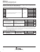
absolute maximum ratings
†
Voltage applied at V
CC
to V
SS
(MSP430C11x1) –0.3 V to 4.6 V. . . . . . . . . . . . . . . . . . . . . . . . . . . . . . . . . . . . . .
Voltage applied at V
CC
to V
SS
(MSP430F11x1) –0.3 V to 4.1 V. . . . . . . . . . . . . . . . . . . . . . . . . . . . . . . . . . . . . . .
Voltage applied to any pin (referenced to V
SS
) –0.3 V to V
CC
+0.3 V. . . . . . . . . . . . . . . . . . . . . . . . . . . . . . . . . . .
Diode current at any device terminal ±2 mA. . . . . . . . . . . . . . . . . . . . . . . . . . . . . . . . . . . . . . . . . . . . . . . . . . . . . . . .
Storage temperature, T
stg
(unprogrammed device) –55°C to 150°C. . . . . . . . . . . . . . . . . . . . . . . . . . . . . . . . . . .
Storage temperature, T
stg
(programmed device) –40°C to 85°C. . . . . . . . . . . . . . . . . . . . . . . . . . . . . . . . . . . . . .
†
Stresses beyond those listed under “absolute maximum ratings” may cause permanent damage to the device. These are stress ratings only, and
functional operation of the device at these or any other conditions beyond those indicated under “recommended operating conditions” is not
implied. Exposure to absolute-maximum-rated conditions for extended periods may affect device reliability.
NOTE: All voltages referenced to V
SS
.
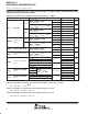
recommended operating conditions
MIN NOM MAX UNITS
MSP430C11x1
18
36
Su
pp
ly voltage during
p
rogram execution V
CC
(see Note 5)
MSP430C11
x
1
1
.
8
3
.
6
V
Su ly
voltage
during
rogram
execution
,
V
CC
(see
Note
5)
MSP430F11x1 1.8 3.6
V
Supply voltage during program/erase flash memory, V
CC
MSP430F11x1 2.7 3.6 V
Supply voltage, V
SS
0 V
Operating free-air temperature range, T
A
MSP430x11x1 –40 85 °C
LFXT1 t l f
LF mode selected, XTS=0 Watch crystal 32768 Hz
LFXT1 crystal frequency,
f
(LFXT1)
(see Note 6)
XT1 mode selected XTS=1
Ceramic resonator 450 8000
kHz
f
(LFXT1)
(see
Note
6)
XT1
mode
selected
,
XTS
=
1
Crystal 1000 8000
kH
z
V
CC
= 1.8 V,
MSP430x11x1
dc 2
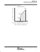
Processor frequency f
(system)
(MCLK signal)
V
CC
= 2.2 V,
MSP430x11x1
dc 5
MHz
V
CC
= 3.6 V,
MSP430x11x1
dc 8
Flash timing generator frequency, f
(FTG)
MSP430F11x1 257 476 kHz
Cumulative program time, segment write, t
(CPT)
(see Note 7)
V
CC
= 2.7 V/3.6 V
MSP430F11x1
3 ms
Low-level input voltage (TCK, TMS, TDI, RST/NMI), V
IL
(excluding XIN, XOUT)
V
CC
= 2.2 V/3 V V
SS
V
SS
+0.6 V
High-level input voltage (TCK, TMS, TDI, RST/NMI), V
IH
(excluding XIN, XOUT)
V
CC
= 2.2 V/3 V 0.8V
CC
V
CC
V
In
p
ut levels at XIN XOUT
V
IL(XIN,
XOUT)
V
CC
= 2 2 V/3 V
V
SS
0.2×V
CC
V
Inp
u
t
le
v
els
at
XIN
,
XOUT
V
IH(XIN,
XOUT)
V
CC
=
2
.
2
V/3
V
0.8×V
CC
V
CC
V
NOTES: 5. The LFXT1 oscillator in LF-mode requires a resistor of 5.1 MΩ from XOUT to VSS when VCC <2.5 V.
The LFXT1 oscillator in XT1-mode accepts a ceramic resonator or a crystal frequency of 4 MHz at VCC ≥ 2.2 V.
The LFXT1 oscillator in XT1-mode accepts a ceramic resonator or a crystal frequency of 8 MHz at VCC ≥ 2.8 V.
6. The LFXT1 oscillator in LF-mode requires a watch crystal.
The LFXT1 oscillator in XT1-mode accepts a ceramic resonator or a crystal.
7. The cumulative program time must not be exceeded during a segment-write operation.