
Mixed Signal Microcontroller Specification Sheet


MSP430x11x1
MIXED SIGNAL MICROCONTROLLER
SLAS241C – SEPTEMBER 1999 – REVISED JUNE 2000
36
POST OFFICE BOX 655303 • DALLAS, TEXAS 75265
electrical characteristics over recommended ranges of supply voltage and operating free-air
temperature (unless otherwise noted) (continued)
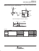
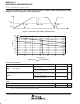
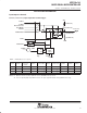
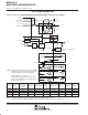
principle characteristics of the DCO
Individual devices have a minimum and maximum operation frequency. The specified parameters for
f
DCOx0
to f
DCOx7
are valid for all devices.
The DCO control bits DCO0, DCO1 and DCO2 have a step size as defined in parameter S
DCO
.
The modulation control bits MOD0 to MOD4 select how often f
DCO+1
is used within the period of 32 DCOCLK
cycles. f
DCO
is used for the remaining cycles. The frequency is an average = f
DCO
× (2
MOD/32
).
The ranges selected by R
Sel4
to R
Sel5
, R
Sel5
to R
Sel6
, and R
Sel6
to R
Sel7
are overlapping.
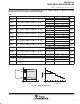
wake-up from lower power modes (LPMx)
PARAMETER TEST CONDITIONS MIN TYP MAX UNIT
t
(LPM0)
V
CC
= 2.2 V/3 V 100
ns
t
(LPM2)
V
CC
= 2.2 V/3 V 100
ns
f
(MCLK)
= 1 MHz, V
CC
= 2.2 V/3 V 6
t
(LPM3)
Delay time (see Note 22)
f
(MCLK)
= 2 MHz, V
CC
= 2.2 V/3 V 6
µs
()
Dela
y
time
(see
Note
22)
f
(MCLK)
= 3 MHz, V
CC
= 2.2 V/3 V 6
f
(MCLK)
= 1 MHz, V
CC
= 2.2 V/3 V 6
t
(LPM4)
f
(MCLK)
= 2 MHz, V
CC
= 2.2 V/3 V 6
µs
()
f
(MCLK)
= 3 MHz, V
CC
= 2.2 V/3 V 6
NOTE 22: Parameter applicable only if DCOCLK is used for MCLK.
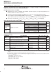
JTAG/programming
PARAMETER TEST CONDITIONS MIN TYP MAX UNIT
f
(TCK)
TCK frequency JTAG/test (see Note 25)
V
CC
= 2.2 V dc 5
MHz
f
(TCK)
TCK
freq
u
enc
y,
JTAG/test
(see
Note
25)
V
CC
= 3 V dc 10
MH
z
V
(FB)
Fuse blow voltage, C versions (see Notes 23 and 24) V
CC
= 2.2 V/3 V 3.5 3.9 V
I
(FB)
Supply current on TDI during fuse blow (see Note 24) (C11x1) 100 mA
t
(FB)
Time to blow the fuse (see Note 24) (C11x1) 1 ms
I
(DD-PGM)
Current during program cycle (see Note 26)
V
CC
= 2.7 V/3.6 V,
MSP430F11x1
3 5 mA
I
(DD-ERASE)
Current during erase cycle (see Note 26)
V
CC
= 2.7 V/3.6 V,
MSP430F11x1
3 5 mA
t
(t ti )
Write/erase cycles MSP430F11x1 10
4
10
5
t
(retention)
Data retention T
J
= 25°C MSP430F11x1 100 Year
NOTES: 23. The power source to blow the fuse is applied to TDI pin.
24. Once the JTAG fuse is blown, no further access to the MSP430 JTAG/test feature is possible. The JTAG block is switched to bypass
mode.
25. f
(TCK)
may be restricted to meet the timing requirements of the module selected.
26. Duration of the program/erase cycle is determined by f
(FTG)
applied to the flash timing controller. It can be calculated as follows:
t
(word
write)
= 35 x 1/f
(FTG)
t
(segment
write,
byte
0)
= 30 × 1/f
(FTG)
t
(segment
write,
byte
1
–
63)
= 20 × 1/f
(FTG)
t
(mass
erase)
= 5297 x 1/f
(FTG)
t
(page
erase)
= 4819 x 1/f
(FTG)