
Mixed Signal Microcontroller Specification Sheet


MSP430x11x1
MIXED SIGNAL MICROCONTROLLER
SLAS241C – SEPTEMBER 1999 – REVISED JUNE 2000
38
POST OFFICE BOX 655303 • DALLAS, TEXAS 75265
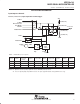
APPLICATION INFORMATION
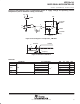
Port P1, P1.4 to P1.7, input/output with Schmitt-trigger and in-system access features
EN
D
See Note 27
See Note 28
See Note 28
See Note 27
GND
V
CC
P1.4–P1.7
0
1
0
1
Interrupt
Edge
Select
EN
Set
Q
P1IE.x
P1IFG.x
P1IRQ.x
Interrupt
Flag
P1IES.x
P1SEL.x
Module X IN
P1IN.x
P1OUT.x
Module X OUT
Direction Control
From Module
P1DIR.x
P1SEL.x
Pad Logic
Bus Keeper
TST
Fuse
60 kΩ
Fuse
Blow
Control
Control By JTAG
0
1
TDO
Controlled By JTAG
P1.x
TDI
P1.x
TST
TST
TMS
TST
TCK
TST
Controlled by JTAG
TST
P1.x
P1.x
NOTE: The test pin should be protected from potential EMI
and ESD voltage spikes. This may require a smaller
external pulldown resistor in some applications.
x = Bit identifier, 4 to 7 for port P1
During programming activity and during blowing
the fuse, the pin TDO/TDI is used to apply the test
input for JTAG circuitry.
P1.7/TDI/TDO
P1.6/TDI
P1.5/TMS
P1.4/TCK
Typical
TEST
GND
NOTE: Fuse not implemented
in F11x1
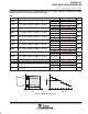
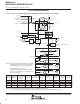
PnSel.x PnDIR.x
Direction
control from
module
PnOUT.x Module X OUT PnIN.x Module X IN PnIE.x PnIFG.x PnIES.x
P1Sel.4 P1DIR.4 P1DIR.4 P1OUT.4 SMCLK P1IN.4 unused P1IE.4 P1IFG.4 P1IES.4
P1Sel.5 P1DIR.5 P1DIR.5 P1OUT.5 Out0 signal
†
P1IN.5 unused P1IE.5 P1IFG.5 P1IES.5
P1Sel.6 P1DIR.6 P1DIR.6 P1OUT.6 Out1 signal
†
P1IN.6 unused P1IE.6 P1IFG.6 P1IES.6
P1Sel.7 P1DIR.7 P1DIR.7 P1OUT.7 Out2 signal
†
P1IN.7 unused P1IE.7 P1IFG.7 P1IES.7
†
Signal from or to Timer_A
NOTES: 27. Optional selection of pullup or pulldown resistors with ROM (masked) versions.
28. Fuses for optional pullup and pulldown resistors can only be programmed at the factory (ROM versions only).