TMS320DM644x DMSoC VLYNQ Port User's Guide Literature Number: SPRUE36A September 2007
SPRUE36A – September 2007 Submit Documentation Feedback
Contents Preface ............................................................................................................................... 7 1 Introduction................................................................................................................ 9 1.1 Purpose of the Peripheral ....................................................................................... 9 1.2 Features ....................................................................................................
A.2 Supported Ordered Sets ....................................................................................... 40 A.3 VLYNQ 2.0 Packet Format .................................................................................... 41 A.4 VLYNQ 2.X Packets ............................................................................................ 43 .................................................................................. 45 B.1 Write Performance...............................................
List of Figures 1 2 3 4 5 6 7 8 9 10 11 12 13 14 15 16 17 18 19 20 21 22 23 24 25 26 A-1 VLYNQ Port Functional Block Diagram ................................................................................. External Clock Block Diagram ............................................................................................ Internal Clock Block Diagram ............................................................................................. VLYNQ Module Structure ....................................
List of Tables 1 2 3 4 5 6 7 8 9 10 11 12 13 14 15 16 17 18 19 20 21 22 23 24 25 A-1 A-2 A-3 B-1 B-2 B-3 C-1 6 VLYNQ Port Pins ........................................................................................................... Serial Interface Width ...................................................................................................... Address Translation Example (Single Mapped Region) ..............................................................
Preface SPRUE36A – September 2007 Read This First About This Document This document describes the VLYNQ™ communications interface port in the TMS320DM644x Digital Media System-on-Chip (DMSoC). Notational Conventions This document uses the following conventions. • Hexadecimal numbers are shown with the suffix h. For example, the following number is 40 hexadecimal (decimal 64): 40h. • Registers in this document are shown in figures and described in tables.
www.ti.com Related Documentation From Texas Instruments SPRAAA6 — EDMA v3.0 (EDMA3) Migration Guide for TMS320DM644x DMSoC. Describes migrating from the Texas Instruments TMS320C64x digital signal processor (DSP) enhanced direct memory access (EDMA2) to the TMS320DM644x Digital Media System-on-Chip (DMSoC) EDMA3. This document summarizes the key differences between the EDMA3 and the EDMA2 and provides guidance for migrating from EDMA2 to EDMA3. Trademarks VLYNQ is a trademark of Texas Instruments.
User's Guide SPRUE36A – September 2007 VLYNQ Port 1 Introduction 1.1 Purpose of the Peripheral The VLYNQ™ communications interface port is a low pin count, high-speed, point-to-point serial interface in the TMS320DM644x Digital Media System-on-Chip (DMSoC) used for connecting to host processors and other VLYNQ-compatible devices. The VLYNQ port is a full-duplex serial bus where transmit and receive operations occur separately and simultaneously without interference.
www.ti.com Introduction • • • • • • 1.3 Symmetric Operations – Transmit (TX) pins on the first device connect to the receive (RX) pins on the second device and vice-versa. – Data pin widths are automatically detected after reset – Re-request packets, response packets, and flow control information are all multiplexed and sent across the same physical pins.
www.ti.com Peripheral Architecture 2 Peripheral Architecture This section discusses the architecture and basic functions of the VLYNQ peripheral. 2.1 Clock Control The module's serial clock direction and frequency are software configurable through the CLKDIR and CLKDIV bits in the VLYNQ control register (CTRL). The VLYNQ serial clock can be sourced from the internal system clock (CLKDIR = 1) or by an external clock source (CLKDIR = 0) for its serial operations.
www.ti.com Peripheral Architecture 2.2 Signal Descriptions The VLYNQ module on the DM644x device is configurable for a 1 to 4 bit-wide RX/TX. Chip-level pin multiplexing registers control the configuration. See the pin multiplexing information in the device-specific data manual. If the configured width does not match the number of transmit/receive lines that are available on the remote device, negotiation between the two VLYNQ devices automatically configures the width (see Section 2.7).
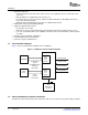
www.ti.com Peripheral Architecture 2.5 VLYNQ Functional Description The VLYNQ core supports both host-to-peripheral and peer-to-peer communication models and is symmetrical. The VLYNQ module structure is shown in Figure 4. Figure 4.
www.ti.com Peripheral Architecture 2.5.1 Write Operations Write requests that initiate from the slave configuration bus interface of the local device write to the outbound command (CMD) FIFO. Data is subsequently read from the FIFO and encapsulated in a write request packet. The address is translated, and the packet is encoded and serialized before being transmitted to remote device. The remote device subsequently deserializes and decodes the receive data and writes it into the inbound CMD FIFO.
www.ti.com Peripheral Architecture 2.5.2 Read Operations Read requests from the slave configuration bus interface are written to the outbound CMD FIFO (similar to the write requests). Data is subsequently read from the FIFO and encapsulated into a read request packet. The packet is encoded and serialized before it is transmitted to the remote device. Next, the remote device deserializes, decodes the receive data, and writes the receive data to the inbound CMD FIFO.
www.ti.com Peripheral Architecture Note: Not servicing read operations results in deadlock. The only way to recover from a deadlock situation is to perform a hard reset. Read operations are typically not serviced due to read requests that are issued to a non-existent remote VLYNQ device or they are not serviced due to trying to perform reads on the VLYNQ memory map prior to establishing the link.
www.ti.com Peripheral Architecture 2.9 Address Translation Remote VLYNQ device(s) are memory mapped to the local (host) device’s address space when a link is established (this is similar to any other on-chip peripherals). Enumerating the VLYNQ devices (single or multiple) into a coherent memory map for accessing each device is part of the initialization sequence. After the enumeration, the host (local) device can access the remote device address map using local device addresses.
www.ti.com Peripheral Architecture Figure 7. Example Address Memory Map DMxxx device (local) Remote VLYNQ device 0000:0000 Map region 1 0400:0000 (0C00:0000 on CONFIG bus) 03FF:FFFF 0400:0000 Map region 1 Map region 2 07FF:FFFF 0800:0000 0800:00FF 0800:0100 0400:00FF Map region 2 0500:0000 Map region 3 Map region 3 0801:00FF 0801:0100 0500:FFFF Map region 4 0B00:0000 Map region 4 0841:00FF 0B3F:FFFF The following shows an example illustrating the address translation used in each VLYNQ module.
www.ti.
www.ti.com Peripheral Architecture Example 1. Address Translation Example The remote address 0x 0400 : 0154 (or 0x0000 0054) was translated to 0x 8200 : 0054 on the DM644x (local) device in this example.
www.ti.com Peripheral Architecture 2.11 Reset Considerations 2.11.1 Software Reset Considerations Peripheral clock and reset control is done through the power and sleep controller (PSC) module that is included with the device. For more information, refer to the power management section (Section 2.14). Additionally, there is a software reset (the reset bit in the VLYNQ control register, CTRL) within the peripheral itself.
www.ti.com Peripheral Architecture Figure 8.
www.ti.com Peripheral Architecture 2.12.3 Remote Interrupts Remote interrupts occur when an interrupt packet is received over the serial interface from a remote device. The interrupt status is extracted from the packet and written to a location pointed to by the interrupt pointer register (INTPTR). The INTPTR should contain the address of the interrupt pending/set register (INTPENDSET). To get INTPTR to contain the address of INTPENDSET, program INTPTR with a value of 14h (the offset for INTPENDSET).
www.ti.com Peripheral Architecture 2.14 Power Management The VLYNQ module can be placed in reduced-power modes to conserve power during periods of low activity. The power management of the peripheral is controlled by the processor Power and Sleep Controller (PSC). The PSC acts as a master controller for power management of all of the peripherals on the processor.
www.ti.com VLYNQ Port Registers 3 VLYNQ Port Registers Table 5 describes the address space for the VLYNQ registers and memory. Table 5. VLYNQ Register Address Space Block Name Start Address End Address Size VLYNQ Control Registers 01E0 1000h 01E0 11FFh 512 bytes Reserved 01E0 1200h 01E0 1FFFh - VLYNQ Remote Memory Map 0C00 0000h 0CFF FFFFh 64 Mbytes Table 6 lists the memory-mapped registers for the VLYNQ port controller.
www.ti.com VLYNQ Port Registers 3.1 Revision Register (REVID) The revision register (REVID) contains the major and minor revisions for the VLYNQ module. The REVID is shown in Figure 9 and described in Table 7. Figure 9. Revision Register (REVID) 31 16 ID R-1h 15 8 7 0 REVMAJ REVMIN R-2h R-6h LEGEND: R = Read only; -n = value after reset Table 7.
www.ti.com VLYNQ Port Registers 3.2 Control Register (CTRL) The control register (CTRL) determines operation of the VLYNQ module. The CTRL is shown in Figure 10 and described in Table 8. Figure 10.
www.ti.com VLYNQ Port Registers Table 8. Control Register (CTRL) Field Descriptions (continued) Bit 7 6-3 2 1 0 28 Field Value INT2CFG Reserved Interrupt to configuration register. Determines which register is written with the status contained in interrupt packets that are received over the serial interface. Always write 1 to this bit and configure the interrupt pointer register to point to the interrupt pending/set register.
www.ti.com VLYNQ Port Registers 3.3 Status Register (STAT) The status register (STAT) is used to detect conditions that may be of interest to the system designer. The STAT is shown in Figure 11 and described in Table 9. Figure 11.
www.ti.com VLYNQ Port Registers Table 9. Status Register (STAT) Field Descriptions (continued) Bit 8 Field Value RERROR Description Remote Error. Write a 1 to this bit to clear it. 0 No error 1 This bit indicates that a downstream VLYNQ module has detected a packet error. This bit is set when an error indication, /E/, is received from the serial interface. See Appendix A. If this bit is set, and the INTENABLE (bit 13 in VLYNQ control register) is also set, it asserts the VLYNQ interrupt (VLQINT).
www.ti.com VLYNQ Port Registers 3.4 Interrupt Priority Vector Status/Clear Register (INTPRI) The interrupt priority vector status/clear register (INTPRI) displays the highest priority vector with a pending interrupt when read. When writing, only bits [4:0] are valid, and the value represents the vector of the interrupt to be cleared. The INTPRI is shown in Figure 12 and described in Table 10. Figure 12.
www.ti.com VLYNQ Port Registers 3.6 Interrupt Pending/Set Register (INTPENDSET) The interrupt pending/set register (INTPENDSET) indicates the pending interrupt status when the INTLOCAL bit in the control register (CTRL) is not set. When the interrupt packet is forwarded on the serial interface, these bits are cleared. The INTPENDSET is shown in Figure 14 and described in Table 12. Figure 14.
www.ti.com VLYNQ Port Registers 3.8 Transmit Address Map Register (XAM) The transmit address map register (XAM) is used to translate transmit packet addresses to remote device configuration bus addresses. The XAM is shown in Figure 16 and described in Table 14. Figure 16. Transmit Address Map Register (XAM) 31 2 1 0 TXADRMAP Reserved R/W-0 R-0 LEGEND: R/W = Read/Write; R = Read only; -n = value after reset Table 14.
www.ti.com VLYNQ Port Registers 3.9 Receive Address Map Size 1 Register (RAMS1) The receive address map size 1 register (RAMS1) is used to identify the intended destination of inbound serial packets. The RAMS1 is shown in Figure 17 and described in Table 15. Figure 17. Receive Address Map Size 1 Register (RAMS1) 31 2 1 0 RXADRSIZE1 Reserved R/W-0 R-0 LEGEND: R/W = Read/Write; R = Read only; -n = value after reset Table 15.
www.ti.com VLYNQ Port Registers 3.11 Receive Address Map Size 2 Register (RAMS2) The receive address map size 2 register (RAMS2) is used to identify the intended destination of inbound serial packets. The RAMS2 is shown in Figure 19 and described in Table 17. Figure 19. Receive Address Map Size 2 Register (RAMS2) 31 2 1 0 RXADRSIZE2 Reserved R/W-0 R-0 LEGEND: R/W = Read/Write; R = Read only; -n = value after reset Table 17.
www.ti.com VLYNQ Port Registers 3.13 Receive Address Map Size 3 Register (RAMS3) The receive address map size 3 register (RAMS3) is used to identify the intended destination of inbound serial packets. The RAMS3 is shown in Figure 21 and described in Table 19. Figure 21. Receive Address Map Size 3 Register (RAMS3) 31 2 1 0 RXADRSIZE3 Reserved R/W-0 R-0 LEGEND: R/W = Read/Write; R = Read only; -n = value after reset Table 19.
www.ti.com VLYNQ Port Registers 3.15 Receive Address Map Size 4 Register (RAMS4) The receive address map size 4 register (RAMS4) is used to identify the intended destination of inbound serial packets. The RAMS4 is shown in Figure 23 and described in Table 21. Figure 23. Receive Address Map Size 4 Register (RAMS4) 31 2 1 0 RXADRSIZE4 Reserved R/W-0 R-0 LEGEND: R/W = Read/Write; R = Read only; -n = value after reset Table 21.
www.ti.com VLYNQ Port Registers 3.17 Chip Version Register (CHIPVER) VLYNQ allows inter-connection of many VLYNQ devices. In order for software to control the device functions, there must be a mechanism that allows the software to identify VLYNQ devices. Each device that has a VLYNQ module in it has a unique device ID associated with it, which is software readable via a memory-mapped register within the VLYNQ module called the chip version register (CHIPVER).
www.ti.com Remote Configuration Registers 4 Remote Configuration Registers The remote configuration registers listed in Table 25 are the same registers as previously described, but they are for the remote VLYNQ device. Note: Before attempting to access the remote registers (offsets 80h through C0h) , you must ensure that a link is established with the remote device. Poll the LINK bit in the VLYNQ status register (STAT) to do this.
www.ti.com Appendix A Appendix A VLYNQ Protocol Specifications VLYNQ relies on 8b/10b block coding to minimize the number of serial pins and allow for in-band packet delineation and control. The following sections include general 8b/10b coding definitions and their implementation. A.1 Special 8b/10b Code Groups Table A-1. Special 8b/10b Code Groups A.2 Code Group Name Octet Value Octet Bits Current RD - Current RD + K28.0 1C 0001 1100 001111 0100 110000 1011 K28.
www.ti.com VLYNQ 2.0 Packet Format A.2.1 Idle (/I/) The idle ordered sets are transmitted continuously and repetitively whenever the serial interface is idle. Idle is also used in the place of the flowed code in VLYNQ versions 2.0 and later. A.2.2 End of Packet (/T/) An end of packet delimiter delineates the ending boundary of a packet. A.2.3 Byte Disable (/M/) The byte disable symbol masks bytes for write operations. A.2.
www.ti.com VLYNQ 2.0 Packet Format Table A-3. Packet Format (10-bit Symbol Representation) Description Field Value Description PKTTYPE[3:0] This field indicates the packet type. 0000 Reserved 0001 Write with address increment. 0010 Reserved 0011 Write 32-bit word with address increment. 0100 Reserved 0101 Configuration write with address increment. 0110 Reserved for extended command indicator (cmd2). 0111 Interrupt 1000 Reserved 1001 Read with address increment.
www.ti.com VLYNQ 2.X Packets A.4 VLYNQ 2.X Packets An example of what can happen to a write burst due to remote and local FIFO state changes and the link pulse timer expiring is shown in Example A-1. This protocol can be extended to apply to multiple channels; therefore, the data return channel is logically isolated from the command channel. Example A-1.
www.ti.com VLYNQ 2.X Packets A command, length, address, and start receive data from the idle stream. A flow enable was received for the command channel, but there is data to return, so the flow is followed by a channel 1 descriptor (the command for return data actually indicates a channel 1), and the channel 1 packet is now under way. A flow is now received for channel 1, but it is soon disabled so the channel 1 packet continues.
www.ti.com Appendix B Appendix B Write/Read Performance The following sections discuss the write versus read performance and how the throughput (read or write) should be calculated for a given data width and serial clock frequency. Note: B.1 The data and throughput calculations shown here are sample calculations for most ideal situations.
www.ti.com Write Performance Table B-1. Scaling Factors Burst Size in 32-bit words Data Bytes Overhead Bytes Scaling Factor 1 4 6 40% 4 16 7 69.56% 8 32 7 82.05% 16 64 7 90.14% Table B-2. Expected Throughput (VLYNQ Interface Running at 76.5 MHZ and 99 MHZ) Interface Running at 99 MHZ Number of VLYNQ Pins Mbits/sec Mbytes/sec Mbits/sec Mbytes/sec 1 1 24.19 3.02 31.68 3.96 4 42.07 5.26 55.09 6.89 2 3 4 46 Interface Running at 76.
www.ti.com Read Performance B.2 Read Performance Since reads must complete a transmit-remote read-receive cycle before starting another read transaction, the data throughput is lower as compared to writes. There is latency involved in reading the data from the remote device; and in some cases, a local latency in writing the returned data before the next read can start. The max read rate is calculated the same way as the max write rate.
www.ti.com Appendix C Appendix C Revision History Table C-1 lists the changes made since the previous version of this document. Table C-1. Document Revision History Reference Additions/Modifications/Deletions Section 2.9 Changed fourth paragraph. Added NOTE. Table 8 Section 3.17 Changed Description of INTLOCAL. Changed paragraph. Figure 25 Changed DEVID reset value. Table 23 Changed DEVID Description. Figure A-1 Changed figure. Table A-3 Changed Description of PKTTYPE[3:0] = 0110.
IMPORTANT NOTICE Texas Instruments Incorporated and its subsidiaries (TI) reserve the right to make corrections, modifications, enhancements, improvements, and other changes to its products and services at any time and to discontinue any product or service without notice. Customers should obtain the latest relevant information before placing orders and should verify that such information is current and complete.