
User manual


www.ti.com
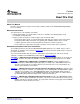
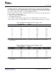
DSP Subsystem
SYSCLK1
SYSCLK3
SCR
EDMA
DDR2 PHY
DDR2 VTP
DDR2 Mem Ctlr
PLLDIV1 (/2)
BPDIV
PLL Controller 2
PLL Controller 1
PLLDIV2 (/3)
PLLDIV3 (/6)
PLLDIV1 (/1)
SYSCLK2
UARTs (x2)
I2C
Timers (x3)
PWMs (x3)
EMAC
EMIFA
VLYNQ
HPI
McASP0
McBSP0
GPIO
McBSP1
PCI
MXI/CLKIN
(15−30 MHz)
OSCDIV1 (/1)
OBSCLK
(CLKOUT0 Pin)
AUXCLK
Device Clocking
Modules in the CLKDIV6 domain (for example, CLKDIV6 domain peripherals) must run at 1/6 the DSP
frequency.
Modules in the CLKIN domain (for example, UART, Timer, I2C, PWM) run at the MXI/CLKIN frequency,
asynchronous to the DSP. There is no fixed ratio requirement between these peripherals frequencies and
the DSP frequency.
Refer to device-specific data manual for the core clock domain for each peripheral.
Figure 1. Overall Clocking Diagram
SPRUES0B – December 2007 Phase-Locked Loop Controller (PLLC) 7
Submit Documentation Feedback