Universal Operational Amplifier Evaluation Module With Shutdown User’s Guide 1998 Mixed-Signal Products SLVU009
IMPORTANT NOTICE Texas Instruments and its subsidiaries (TI) reserve the right to make changes to their products or to discontinue any product or service without notice, and advise customers to obtain the latest version of relevant information to verify, before placing orders, that information being relied on is current and complete.
How to Use This Manual Preface Read This First About This Manual This User’s Guide describes the universal operational amplifier (op amp) evaluation module (EVM) with shutdown that can be used to construct many op amp evaluation circuits. Schematics of the EVM and several example circuits are included.
iv
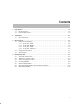
Running Title—Attribute Reference Contents 1 Introduction . . . . . . . . . . . . . . . . . . . . . . . . . . . . . . . . . . . . . . . . . . . . . . . . . . . . . . . . . . . . . . . . . . . . . 1-1 1.1 Design Features . . . . . . . . . . . . . . . . . . . . . . . . . . . . . . . . . . . . . . . . . . . . . . . . . . . . . . . . . . . . 1-2 1.2 Power Requirements . . . . . . . . . . . . . . . . . . . . . . . . . . . . . . . . . . . . . . . . . . . . . . . . . . . . . . . . 1-2 2 Schematics . . . . . .
Running Title—Attribute Reference Figures 2–1 2–2 2–3 2–4 3–1 3–2 3–3 4–1 4–2 4–3 4–4 4–5 4–6 vi Area 100 Schematic – SOIC (14 pin) . . . . . . . . . . . . . . . . . . . . . . . . . . . . . . . . . . . . . . . . . . . . 2-2 Area 200 Schematic – MSOP (10 pin) . . . . . . . . . . . . . . . . . . . . . . . . . . . . . . . . . . . . . . . . . . . 2-3 Area 300 Schematic – SOIC (8 pin) . . . . . . . . . . . . . . . . . . . . . . . . . . . . . . . . . . . . . . . . . . . . .
Chapter 1 Introduction This User’s Guide describes a universal operational amplifier (op amp) evaluation module (EVM) with shutdown (#SLOP224). The EVM simplifies evaluation of Texas Instruments surface-mount op amps with the shutdown feature. Topic Page 1.1 Design Features . . . . . . . . . . . . . . . . . . . . . . . . . . . . . . . . . . . . . . . . . . . . . . 1–2 1.2 Power Requirements . . . . . . . . . . . . . . . . . . . . . . . . . . . . . . . . . . . . . . . . . .
Design Features 1.1 Design Features The board design allows many circuits to be constructed easily and quickly. The board has four circuit development areas that can be snapped apart. Areas 100 and 200 are for dual op amps in the SOIC and MSOP packages. Area 300 is for single op amps in SOIC packages. Area 400 is for single op amps in SOT23-6 packages.
Chapter 2 Schematics This chapter contains schematics and pin-outs for each of the four areas. Topic 2.1 Page Area Schematics . . . . . . . . . . . . . . . . . . . . . . . . . . . . . . . . . . . . . . . . . . . . . .
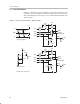
Area Schematics 2.1 Area Schematics Figures 2–1 through 2–4 show schematics for each of the board areas. The schematics show all components that the board layout can accommodate. These should only be used as reference, since not all components will be used at any one time. Figure 2–1.
Area Schematics Figure 2–2.
Area Schematics Figure 2–3. Area 300 Schematic – SOIC (8 pin) C301 R301 V3+ V3+ R303 C304 301– C303 V3+ R304 302– GND3 C305 R302 C302 C306 R308 2 R307 303+ V3– 7 8 – 6 3 + 4 R309 304+ Power Supply Bypass 3/SD 3OUT U301 V3– V3– R305 3 FLT R306 C309 C307 V3+ R312 C308 VREF3 R311 R C310 C U302 A U301 pins 1 and 5 = NC R310 Voltage Reference Figure 2–4.
Chapter 3 Board Layout This chapter shows the universal op amp EVM with shutdown board layout, and describes the relationships between the four areas. Topic Page 3.1 Physical Consideration . . . . . . . . . . . . . . . . . . . . . . . . . . . . . . . . . . . . . . . . 3–2 3.2 Component Placement . . . . . . . . . . . . . . . . . . . . . . . . . . . . . . . . . . . . . . . . 3–3 3.3 Board Layout . . . . . . . . . . . . . . . . . . . . . . . . . . . . . . . . . . . . . . . . . . . . . . . . .
Physical Considerations 3.1 Physical Considerations The EVM board has four circuit development areas. Each area can be separated from the others by breaking along the score lines. The circuit layout in each area supports an op amp package, voltage reference, and ancillary devices. The op amp package is unique to each area as described in the following paragraphs. The voltage reference and supporting devices are the same for all areas.
Component Placement 3.2 Component Placement Figure 3–1 shows component placement for the EVM board. Figure 3–1.
Board Layout 3.3 Board Layout Figures 3–2 and 3–3 show the EVM top and bottom board layouts, respectively. Figure 3–2.
Board Layout Figure 3–3.
3-6 Board Layout
Chapter 4 Example Circuits This chapter shows and discusses several example circuits that can be constructed using the universal operational amplifier EVM. The circuits are all classic designs that can be found in most operational amplifier design books. Topic Page 4.1 Schematic Conventions . . . . . . . . . . . . . . . . . . . . . . . . . . . . . . . . . . . . . . . 4–2 4.2 Sallen-Key Low-Pass Filter . . . . . . . . . . . . . . . . . . . . . . . . . . . . . . . . . . . . 4–3 4.
Schematic Conventions 4.1 Schematic Conventions Figures 4–1 through 4–6 show schematic examples of circuits that can be constructed using the universal operational amplifier EVM with shutdown. The components that are placed on the board are shown in bold. Unused components are blanked out. Jumpers and other changes are noted. These examples are only a few of the many circuits that can be built.
Sallen-Key Low-Pass Filter 4.2 Sallen-Key Low-Pass Filter Figure 4–1 shows area 100 equipped with a dual operational amplifier configured as a second-order Sallen-Key low-pass filter using dual-power supplies. Basic setup is done by proper choice of resistors R and mR, and capacitors C and nC. The transfer function is: V OUT V IN Where: + 1 ǒ ń Ǔ ) ǒjńQǓǒfńfoǓ 1 – f fo 2 fo + 2p Ǹm1 n RC Q + mǸm) n1 And Figure 4–1.
Sallen-Key High-Pass Filter 4.3 Sallen-Key High-Pass Filter Figure 4–2 shows area 200 equipped with a dual operational amplifier configured as a second-order Sallen-Key high-pass filter using single-supply power input. Basic setup is done by proper choice of resistors R and mR, and capacitors C and nC. Note that capacitors should be used for components R211 and R212, and a resistor for C201.
Sallen-Key High-Pass Filter Figure 4–2. Sallen-Key High-Pass Filter with Single Supply Using Area 200 R219 C206 V2+ R206 R221 Jumper C204 0.1 µF C205 10 µF R210 A202– R209 R220 A203+ C212 C213 R208 A204+ Power Supply Bypass A2/SD A2OUT 1/2 Dual Op Amp Not Used V2– Jumper V1– Jumper V2+ 5 10 2 – 1 3 + U201a 4 A201– V2+ GND2 C215 V2– C214 R218 R207 A2 FLT C207 C208 R213 R204 VREF2 = 2.5 V R203 C209 R202 R215 Jumper 2.
Inverting Amplifier 4.4 Inverting Amplifier Figure 4–3 shows area 300 equipped with a single operational amplifier configured as an inverting amplifier using dual power supplies. Basic setup is done by choice of input and feedback resistors. The transfer function for the circuit as shown is: V OUT + –VIN RR302 304 To cancel the effects of input bias current, set R306 = R302 || R304, or use a 0-Ω jumper for R306 if the operational amplifier is a low input bias operational amplifier. Figure 4–3.
Noninverting Amplifier 4.5 Noninverting Amplifier Figure 4–4 shows area 400 equipped with a single operational amplifier configured as a noninverting amplifier with single-supply power input. Basic setup is done by choice of input and feedback resistors. The transfer function for the circuit as shown is: V OUT ǒ Ǔ + VIN 1 ) RR402 ) VREF4 404 The input signal must be referenced to VREF4.
Two Operational Amplifier Instrumentation Amplifier 4.6 Two Operational Amplifier Instrumentation Amplifier Figure 4–5 shows area 200 equipped with a dual operational amplifier configured as a two-operational-amplifier instrumentation amplifier using a voltage reference and single power supply. Basic setup is done by choice of input and feedback resistors.
Two Operational Amplifier Instrumentation Amplifier Figure 4–5. Two Operational Amplifier Instrumentation Amplifier with Single Supply Using Area 200 C206 R219 Jumper A201 – to B2OUT R206 R221 R208 = R206 II R210 or Short if Using Low Input Bias Op Amp C215 Jumper R210 A202– V2+ R209 V1– 10 5 – 1 3 + U201a 4 R220 R208 A204+ Jumper GND2 V2+ 2 A203+ V2+ C204 0.
Differential Amplifier 4.7 Differential Amplifier Figure 4–6 shows area 300 equipped with a single operational amplifier configured as a differential amplifier using a voltage reference and single power supply. Basic setup is done by choice of input and feedback resistors.