
Datasheet


Area Schematics
2-2
Schematics
2.1 Area Schematics
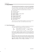
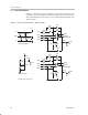
Figures 2–1 through 2–4 show schematics for each of the board areas. The
schematics show all components that the board layout can accommodate.
These should only be used as reference, since not all components will be used
at any one time.
Figure 2–1. Area 100 Schematic – SOIC (14 pin)
C104 C105
C112 C113
V1+
V1–
V1+
GND1
V1–
Power Supply Bypass
+
–
14
1
4
3
2
V1+
V1–
R106
C115
R119
C106
R121
R110
R120
R109
R108
R118C114
C107
A1OUT
1/2 Dual Op Amp
A101–
A102–
A103+
A104+
+
–
13
11
12
R104
C109
R113
C102
R103
R102
R112
R101
R111
R114
C110
C101
B1OUT
1/2 Dual Op Amp
B101–
B102–
B103+
B104+
R116
C
R
A
U102
R117
Voltage Reference
V1+
VREF1
U101a
U101b
R115
A1/SD
C108
R107
A1 FLT
B1/SD
9
C103
R105
B1 FLT
C111
U101 pins 5, 7, 8, and 10 = NC
6