
Datasheet


Design Features
1-2
Introduction
1.1 Design Features
The board design allows many circuits to be constructed easily and quickly.
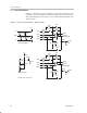
The board has four circuit development areas that can be snapped apart.
Areas 100 and 200 are for dual op amps in the SOIC and MSOP packages.
Area 300 is for single op amps in SOIC packages. Area 400 is for single op
amps in SOT23-6 packages. A few possible circuits are as follows:
Voltage follower
Noninverting amplifier
Inverting amplifier
Simple or algebraic summing amplifier
Difference amplifier
Current to voltage converter
Voltage to current converter
Integrator/low-pass filter
Differentiator/high-pass filter
Instrumentation amplifier
Sallen-Key filter
Two-layer board construction with a ground plane on the solder side ensures
that circuit performance will be on par with final production designs.
1.2 Power Requirements
The devices and designs that are used dictate the input power requirements.
Three input terminals are provided for each area of the board:
Vx+ Positive input power for area x00 i.e., V1+ ⇒ area 100
GNDx Ground reference for area x00 i.e., GND2 ⇒ area 200
Vx– Negative input power for area x00 i.e., V4– ⇒ area 400
Each area has four bypass capacitors – two for the positive supply, and two
for the negative supply. Each supply should have a 1-µF to 10-µF capacitor for
low frequency bypassing and a 0.01-µF to 0.1-µF capacitor for high frequency
bypassing.
When using single-supply circuits, the negative supply is shorted to ground by
bridging C112 or C113 in area 100, C212 or C213 in area 200, C305 or C306
in area 300, or C405 or C406 in area 400. Power input is between Vx+ and
GNDx. The voltage reference circuitry is provided for single-supply
applications that require a reference voltage to be generated.