
Computer Hardware User Manual


PCI445X Buffer Types
C-2
C.1 PCI445X Buffer Types
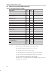
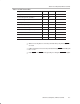
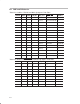
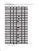
Table C–1. PCI445X Terminal Function Assignment and Buffer Types
Signal Name Terminal Type Signal Name Terminal Type
A_CAD0 B8 TS A_CAD28 N2 TS
A_CAD1 A7 TS A_CAD29 N3 TS
A_CAD2 C8 TS A_CAD30 P1 TS
A_CAD3 A6 TS A_CAD31 D9 TS
A_CAD4 B7 TS A_CAUDIO M1 I
A_CAD5 B6 TS A_CBLOCK D2 P
A_CAD6 C7 TS A_CC/BE0 A4 TS
A_CAD7 D7 TS A_CC/BE1 C3 TS
A_CAD8 C6 TSO A_CC/BE2 F2 TS
A_CAD9 C5 TS A_CC/BE3 J1 TS
A_CAD10 B4 TS A_CCD1 A8 I
A_CAD11 A3 TS A_CCD2 M4 TS
A_CAD12 C4 TS A_CCLK E3 TS
A_CAD13 D5 TS A_CLKRUN M3 STS
A_CAD14 B2 TS A_CDEVSEL D1 STS
A_CAD15 B3 TS A_CFRAME G4 STS
A_CAD16 A2 TS A_CGNT C1 STS
A_CAD17 F1 TS A_CINT L2 I
A_CAD18 G3 TS A_CIRDY E1 STS
A_CAD19 G2 P A_CPAR C2 TS
A_CAD20 H3 TS A_CPERR D3 STS
A_CAD21 H1 TS A_CREQ J3 I
A_CAD22 J4 TS A_CRST H2 O
A_CAD23 J2 TS A_CSERR L3 I
A_CAD24 K2 TS A_CSTOP E4 STS
A_CAD25 K3 TS A_CSTSCHG M2 I
A_CAD26 K1 TS A_CTRDY E2 STS
A_CAD27 N1 TS A_CVS1 L1 I/O
Note: The voltage sense terminals (VS1/CVS1, VS2/CVS2) are always driven low except under the following conditions:
1) High-impedance state during RESET
2) Toggle during socket interrogation