("" "!1 "!-('%& "!# )0$& &%"(#) %& SLES100A − DECEMBER 2003 − REVISED NOVEMBER 2006 FEATURES D 24-Bit Resolution D Analog Performance: D D D D D D − Dynamic Range: 123 dB − THD+N: 0.0005% Differential Current Output: 4 mA p-p 8× Oversampling Digital Filter: − Stop-Band Attenuation: –98 dB − Pass-Band Ripple: ±0.
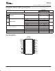
www.ti.com SLES100A − DECEMBER 2003 − REVISED NOVEMBER 2006 ORDERING INFORMATION PRODUCT PACKAGE PACKAGE CODE OPERATION TEMPERATURE RANGE PACKAGE MARKING PCM1796DB 28-lead SSOP 28DB –25°C to 85°C PCM1796 ORDERING NUMBER TRANSPORT MEDIA PCM1796DB Tube PCM1796DBR Tape and reel ABSOLUTE MAXIMUM RATINGS over operating free-air temperature range unless otherwise noted(1) PCM1796 VCC1, VCC2L, VCC2R VDD Supply voltage –0.3 V to 6.5 V –0.3 V to 4 V ±0.
www.ti.com SLES100A − DECEMBER 2003 − REVISED NOVEMBER 2006 ELECTRICAL CHARACTERISTICS (Continued) all specifications at TA = 25°C, VCC1 = VCC2L = VCC2R = 5 V, VDD = 3.3 V, fS = 44.1 kHz, system clock = 256 fS, and 24-bit data unless otherwise noted PCM1796DB PARAMETER TEST CONDITIONS MIN TYP MAX UNIT DIGITAL INPUT/OUTPUT Logic family TTL compatible VIH VIL 2 Input logic level IIH IIL Input logic current VIN = VDD VIN = 0 V VOH VOL Output logic level IOH = –2 mA IOL = 2 mA 0.
www.ti.com SLES100A − DECEMBER 2003 − REVISED NOVEMBER 2006 ELECTRICAL CHARACTERISTICS (Continued) all specifications at TA = 25°C, VCC1 = VCC2L = VCC2R = 5 V, VDD = 3.3 V, fS = 44.1 kHz, system clock = 256 fS, and 24-bit data unless otherwise noted PCM1796DB PARAMETER TEST CONDITIONS MIN TYP UNIT MAX DSD MODE DYNAMIC PERFORMANCE (1) (2) (44.1 kHZ, 64 fS) THD+N at FS 2 V rms Dynamic range –60 dB, EIAJ, A-weighted 0.
www.ti.com SLES100A − DECEMBER 2003 − REVISED NOVEMBER 2006 ELECTRICAL CHARACTERISTICS (Continued) all specifications at TA = 25°C, VCC1 = VCC2L = VCC2R = 5 V, VDD = 3.3 V, fS = 44.1 kHz, system clock = 256 fS, and 24-bit data unless otherwise noted PCM1796DB PARAMETER TEST CONDITIONS MIN TYP UNIT MAX POWER SUPPLY REQUIREMENTS VDD VCC1 VCC2L VCC2R Voltage range 3 3.3 3.6 VDC 4.75 5 5.25 VDC 7 9 fS = 44.
www.ti.
www.ti.
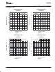
www.ti.com SLES100A − DECEMBER 2003 − REVISED NOVEMBER 2006 TYPICAL PERFORMANCE CURVES DIGITAL FILTER Digital Filter Response AMPLITUDE vs FREQUENCY AMPLITUDE vs FREQUENCY 0 5 0.0005 0.0004 4 −20 3 0.0003 −40 Amplitude – dB Amplitude – dB 2 0.0002 −60 −80 −100 1 0.0001 0 −1 –0.0001 −2 –0.0002 −120 −3 –0.0003 −140 −4 –0.0004 −160 0 1 2 3 4 −5 –0.0005 0.0 0.1 Frequency [× fS] 0.2 0.3 0.4 0.5 Frequency [× fS] Figure 1. Frequency Response, Sharp Rolloff Figure 2.
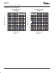
www.ti.com SLES100A − DECEMBER 2003 − REVISED NOVEMBER 2006 De-Emphasis Filter DE-EMPHASIS LEVEL vs FREQUENCY DE-EMPHASIS ERROR vs FREQUENCY 0 0.5 fS = 32 kHz −1 0.3 De-Emphasis Error – dB −2 De-Emphasis Level – dB fS = 32 kHz 0.4 −3 −4 −5 −6 −7 0.2 0.1 −0.0 0.0 −0.1 −0.2 −8 −0.3 −9 −0.4 −10 −0.5 0 2 4 6 8 10 12 14 0 2 4 6 f – Frequency – kHz Figure 5 10 12 14 Figure 6 DE-EMPHASIS LEVEL vs FREQUENCY DE-EMPHASIS ERROR vs FREQUENCY 0 0.5 fS = 44.
www.ti.com SLES100A − DECEMBER 2003 − REVISED NOVEMBER 2006 De-Emphasis Filter (Continued) DE-EMPHASIS LEVEL vs FREQUENCY DE-EMPHASIS ERROR vs FREQUENCY 0 0.5 fS = 48 kHz −1 0.3 De-Emphasis Error – dB De-Emphasis Level – dB −2 −3 −4 −5 −6 −7 0.2 0.1 −0.0 0.0 −0.1 −0.2 −8 −0.3 −9 −0.4 −10 −0.5 0 2 4 6 8 10 12 14 f – Frequency – kHz Figure 9 10 fS = 48 kHz 0.
www.ti.com SLES100A − DECEMBER 2003 − REVISED NOVEMBER 2006 ANALOG DYNAMIC PERFORMANCE Supply Voltage Characteristics TOTAL HARMONIC DISTORTION + NOISE vs SUPPLY VOLTAGE DYNAMIC RANGE vs SUPPLY VOLTAGE 126 124 fS = 96 kHz Dynamic Range – dB THD+N – Total Harmonic Distortion + Noise – % 0.01 0.001 fS = 192 kHz fS = 48 kHz 4.75 5.00 5.25 fS = 192 kHz 120 118 fS = 96 kHz 0.0001 4.50 116 4.50 5.50 VCC – Supply Voltage – V 5.00 5.25 5.
www.ti.com SLES100A − DECEMBER 2003 − REVISED NOVEMBER 2006 Temperature Characteristics TOTAL HARMONIC DISTORTION + NOISE vs FREE-AIR TEMPERATURE DYNAMIC RANGE vs FREE-AIR TEMPERATURE 126 124 Dynamic Range – dB THD+N – Total Harmonic Distortion + Noise – % 0.01 fS = 96 kHz 0.001 fS = 192 kHz fS = 48 kHz fS = 96 kHz fS = 48 kHz 122 fS = 192 kHz 120 118 0.
www.ti.com SLES100A − DECEMBER 2003 − REVISED NOVEMBER 2006 AMPLITUDE vs FREQUENCY 0 0 −20 −20 −40 −40 Amplitude – dB Amplitude – dB AMPLITUDE vs FREQUENCY −60 −80 −100 −60 −80 −100 −120 −120 −140 −140 −160 −160 0 2 4 6 8 10 12 14 16 18 20 0 10 20 f – Frequency – kHz 40 50 60 70 80 90 100 f – Frequency – kHz NOTE: PCM mode, fS = 48 kHz, 32768 point 8 average, TA = 25°C, VDD = 3.3 V VCC = 5 V, measurement circuit is Figure 36. Figure 19.
www.ti.com SLES100A − DECEMBER 2003 − REVISED NOVEMBER 2006 SYSTEM CLOCK AND RESET FUNCTIONS System Clock Input The PCM1796 requires a system clock for operating the digital interpolation filters and advanced segment DAC modulators. The system clock is applied at the SCK input (pin 7). The PCM1796 has a system clock detection circuit that automatically senses the frequency at which the system clock is operating. Table 1 shows examples of system clock frequencies for common audio sampling rates.
www.ti.com SLES100A − DECEMBER 2003 − REVISED NOVEMBER 2006 Power-On and External Reset Functions The PCM1796 includes a power-on reset function. Figure 24 shows the operation of this function. With VDD > 2 V, the power-on reset function is enabled. The initialization sequence requires 1024 system clocks from the time VDD > 2 V. After the initialization period, the PCM1796 is set to its default reset state, as described in the MODE CONTROL REGISTERS section of this data sheet.
www.ti.com SLES100A − DECEMBER 2003 − REVISED NOVEMBER 2006 AUDIO DATA INTERFACE Audio Serial Interface The audio interface port is a 3-wire serial port. It includes LRCK (pin 4), BCK (pin 6), and DATA (pin 5). BCK is the serial audio bit clock, and it is used to clock the serial data present on DATA into the serial shift register of the audio interface. Serial data is clocked into the PCM1796 on the rising edge of BCK. LRCK is the serial audio left/right word clock.
www.ti.
www.ti.com SLES100A − DECEMBER 2003 − REVISED NOVEMBER 2006 External Digital Filter Interface and Timing The PCM1796 supports an external digital filter interface comprising a 3- or 4-wire synchronous serial port, which allows the use of an external digital filter. External filters include the Texas Instruments’ DF1704 and DF1706, the Pacific Microsonics PMD200, or a programmable digital signal processor.
www.ti.com SLES100A − DECEMBER 2003 − REVISED NOVEMBER 2006 SERIAL CONTROL INTERFACE The PCM1796 supports SPI and I2C that sets mode control registers as shown in Table 4. This serial control interface is selected by MSEL (pin 3), SPI is activated when MSEL is set to LOW, and I2C is activated when MSEL is set to HIGH. SPI Interface The SPI interface is a 4-wire synchronous serial port that operates asynchronously to the serial audio interface and the system clock (SCK).
www.ti.com SLES100A − DECEMBER 2003 − REVISED NOVEMBER 2006 t(MHH) MS 1.4 V t(MSS) t(MCL) t(MCH) t(MSH) MC 1.4 V t(MCY) LSB MDI t(MDS) 1.
www.ti.com SLES100A − DECEMBER 2003 − REVISED NOVEMBER 2006 I2C INTERFACE The PCM1796 supports the I2C serial bus and the data transmission protocol for standard and fast mode as a slave device. This protocol is explained in I2C specification 2.0. In I2C mode, the control terminals are changed as follows.
www.ti.com SLES100A − DECEMBER 2003 − REVISED NOVEMBER 2006 Write Register A master can write to any PCM1796 registers using single or multiple accesses. The master sends a PCM1796 slave address with a write bit, a register address, and the data. If multiple access is required, the address is that of the starting register, followed by the data to be transferred. When the data are received properly, the index register is incremented by 1 automatically.
www.ti.com SLES100A − DECEMBER 2003 − REVISED NOVEMBER 2006 Noise Suppression The PCM1796 incorporates noise suppression using the system clock (SCK). However, there must be no more than two noise spikes in 600 ns. The noise suppression works for SCK frequencies between 8 MHz and 40 MHz in fast mode. However, it works incorrectly in the following conditions. Case 1: 1. t(SCK) > 120 ns (t(SCK): period of SCK) 2. t(HI) + t(D–HD) < t(SCK) × 5 3.
www.ti.
www.ti.com SLES100A − DECEMBER 2003 − REVISED NOVEMBER 2006 MODE CONTROL REGISTERS User-Programmable Mode Controls The PCM1796 includes a number of user-programmable functions which are accessed via mode control registers. The registers are programmed using the serial control interface, which is previously discussed in the SPI Interface and I2C INTERFACE sections of this data sheet.
www.ti.com SLES100A − DECEMBER 2003 − REVISED NOVEMBER 2006 Register Map The mode control register map is shown in Table 4. Registers 16–21 include an R/W bit, which determines whether a register read (R/W = 1) or write (R/W = 0) operation is performed. Registers 22 and 23 are read-only. Table 4.
www.ti.com SLES100A − DECEMBER 2003 − REVISED NOVEMBER 2006 Register 18 B15 B14 B13 B12 B11 B10 B9 B8 B7 B6 B5 B4 R/W 0 0 1 0 0 1 0 ATLD FMT2 FMT1 FMT0 B3 B2 DMF1 DMF0 B1 B0 DME MUTE R/W: Read/Write Mode Select When R/W = 0, a write operation is performed. When R/W = 1, a read operation is performed. Default value: 0 ATLD: Attenuation Load Control This bit is available for read and write.
www.ti.com SLES100A − DECEMBER 2003 − REVISED NOVEMBER 2006 DME: Digital De-Emphasis Control This bit is available for read and write. Default value: 0 DME = 0 De-emphasis disabled (default) DME = 1 De-emphasis enabled The DME bit is used to enable or disable the de-emphasis function for both channels. MUTE: Soft Mute Control This bit is available for read and write.
www.ti.com SLES100A − DECEMBER 2003 − REVISED NOVEMBER 2006 OPE: DAC Operation Control This bit is available for read and write. Default value: 0 OPE = 0 DAC operation enabled (default) OPE = 1 DAC operation disabled The OPE bit is used to enable or disable the analog output for both channels. Disabling the analog outputs forces them to the bipolar zero level (BPZ) even if audio data is present on the input. DFMS: Stereo DF Bypass Mode Select This bit is available for read and write.
www.ti.com SLES100A − DECEMBER 2003 − REVISED NOVEMBER 2006 SRST: System Reset Control This bit is available for write only. Default value: 0 SRST = 0 Normal operation (default) SRST = 1 System reset operation (generate one reset pulse) The SRST bit is used to reset the PCM1796 to the initial system condition. DSD: DSD Interface Mode Control This bit is available for read and write.
www.ti.com SLES100A − DECEMBER 2003 − REVISED NOVEMBER 2006 OS[1:0]: Delta-Sigma Oversampling Rate Selection These bits are available for read and write. Default value: 00 Operation Speed Select OS[1:0] 00 64 times fS (default) 01 32 times fS 10 128 times fS 11 Reserved The OS bits are used to change the oversampling rate of delta-sigma modulation. Use of this function enables the designer to stabilize the conditions at the post low-pass filter for different sampling rates.
www.ti.com SLES100A − DECEMBER 2003 − REVISED NOVEMBER 2006 ZFGx: Zero-Detection Flag Where x = L or R, corresponding to the DAC output channel. These bits are available only for readback. Default value: 00 ZFGx = 0 Not zero ZFGx = 1 Zero detected These bits show zero conditions. Their status is the same as that of the zero flags at ZEROL (pin 1) and ZEROR (pin 2). See Zero Detect in the FUNCTION DESCRIPTIONS section.
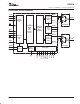
www.ti.com SLES100A − DECEMBER 2003 − REVISED NOVEMBER 2006 APPLICATION INFORMATION TYPICAL CONNECTION DIAGRAM IN PCM MODE Cf 5V Rf 1 ZEROL VCC2L 28 2 ZEROR AGND3L 27 3 MSEL IOUTL– 26 4 LRCK IOUTL+ 25 5 DATA AGND2 24 6 BCK VCC1 23 VCOML 22 VCOMR 21 IREF 20 10 MS AGND1 19 11 MDI IOUTR– 18 12 MC IOUTR+ 17 AGND3R 16 VCC2R 15 + 0.1 µF 10 µF – 7 0.
www.ti.com SLES100A − DECEMBER 2003 − REVISED NOVEMBER 2006 Differential Section The PCM1796 voltage outputs are followed by differential amplifier stages, which sum the differential signals for each channel, creating a single-ended I/V op-amp output. In addition, the differential amplifiers provide a low-pass filter function. The operational amplifier recommended for the differential circuit is the low-noise type. C1 2700 pF R1 820 Ω VCC VCC C11 0.
www.ti.com SLES100A − DECEMBER 2003 − REVISED NOVEMBER 2006 C1 2200 pF R1 820 Ω VCC VCC C11 0.1 µF C17 22 pF 7 IOUT– 5 2 8 – 3 R5 150 Ω 6 + R3 91 Ω R10 120 Ω C3 22000 pF U1 NE5534 4 R8 75 Ω C5 8200 pF C4 27000 pF C15 0.1 µF C19 22 pF 7 2 3 5 – 6 + 4 C12 0.1 µF VEE R4 91 Ω R9 75 Ω R6 150 Ω 8 R11 120 Ω R7 100 Ω U3 NE5534 C16 0.1 µF C6 8200 pF VEE C2 2200 pF R2 820 Ω VCC C13 0.
www.ti.com SLES100A − DECEMBER 2003 − REVISED NOVEMBER 2006 IOUTL– (Pin 26) IOUT– IOUTL+ (Pin 25) IOUT+ Figure 36 Circuit OUT+ 3 1 2 IOUTR– (Pin 18) IOUT– Figure 36 Circuit IOUTR+ (Pin 17) IOUT+ OUT– Balanced Out Figure 38.
www.ti.com SLES100A − DECEMBER 2003 − REVISED NOVEMBER 2006 APPLICATION FOR EXTERNAL DIGITAL FILTER INTERFACE DFMS = 0 External Filter Device PCM1796 1 ZEROL 2 ZEROR 3 MSEL WDCK (Word Clock) 4 LRCK DATA 5 DATA BCK 6 BCK SCK 7 SCK DFMS = 1 External Filter Device PCM1796 DATA_L 1 ZEROL DATA_R 2 ZEROR 3 MSEL 4 LRCK 5 DATA BCK 6 BCK SCK 7 SCK WDCK (Word Clock) Figure 39.
www.ti.com SLES100A − DECEMBER 2003 − REVISED NOVEMBER 2006 Application for Interfacing With an External Digital Filter For some applications, it may be desirable to use an external digital filter to perform the interpolation function, as it can provide improved stop-band attenuation when compared to the internal digital filter of the PCM1796.
www.ti.com SLES100A − DECEMBER 2003 − REVISED NOVEMBER 2006 Audio Format The PCM1796 in the external digital filter interface mode supports right-justified audio formats including 16-bit, 20-bit, and 24-bit audio data, as shown in Figure 40. The audio format is selected by the FMT[2:0] bits of control register18.
www.ti.com SLES100A − DECEMBER 2003 − REVISED NOVEMBER 2006 FUNCTIONS AVAILABLE IN THE EXTERNAL DIGITAL FILTER MODE The external digital filter mode is selected by setting DSD = 0 (register 20, B5) and DFTH = 1 (register 20. B4). The external digital filter mode allows access to the majority of the PCM1796 mode control functions.
www.ti.com SLES100A − DECEMBER 2003 − REVISED NOVEMBER 2006 APPLICATION FOR DSD FORMAT (DSD MODE) INTERFACE DSD Decoder PCM1796 1 ZEROL 2 ZEROR 3 MSEL DATA_R 4 LRCK DATA_L 5 DATA 6 BCK 7 SCK Bit Clock Figure 42. Connection Diagram in DSD Mode Feature This mode is used for interfacing directly to a DSD decoder, which is found in Super Audio CDt (SACD) applications. The DSD mode is accessed by programming the following bit in the corresponding control register.
www.ti.com SLES100A − DECEMBER 2003 − REVISED NOVEMBER 2006 Requirements for System Clock For operation in the DSD mode, the bit clock (DBCK) is required on pin 7 of the PCM1796. The frequency of the bit clock can be N times the sampling frequency. Generally, N is 64 in DSD applications. The interface timing between the bit clock and DSDL and DSDR is required to meet the setup and hold time specifications shown in Figure 44. t = 1/(64 × 44.1 kHz) DBCK DSDL DSDR D0 D1 D2 D3 D4 Figure 43.
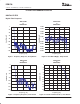
www.ti.com SLES100A − DECEMBER 2003 − REVISED NOVEMBER 2006 ANALOG FIR FILTER PERFORMANCE IN DSD MODE GAIN vs FREQUENCY GAIN vs FREQUENCY 0 0 −1 −10 −2 −20 Gain – dB Gain – dB fc = 185 kHz Gain(1) = –6.6 dB −3 −30 −4 −40 −5 −50 −6 −60 0 50 100 150 200 0 500 f – Frequency – kHz 1000 1500 f – Frequency – kHz Figure 45. DSD Filter-1, Low BW Figure 46.
www.ti.com SLES100A − DECEMBER 2003 − REVISED NOVEMBER 2006 ANALOG FIR FILTER PERFORMANCE IN DSD MODE (CONTINUED) GAIN vs FREQUENCY GAIN vs FREQUENCY 0 0 −1 −10 −2 −20 Gain – dB Gain – dB fc = 85 kHz Gain(1) = –1.5 dB −3 −30 −4 −40 −5 −50 −6 −60 0 50 100 150 200 0 f – Frequency – kHz 500 1000 1500 f – Frequency – kHz Figure 49. DSD Filter-3, Low BW Figure 50.
www.ti.com SLES100A − DECEMBER 2003 − REVISED NOVEMBER 2006 DSD MODE CONFIGURATION AND FUNCTION CONTROLS Configuration for the DSD Interface Mode The DSD interface mode is selected by setting DSD = 1 (register 20, B5).
www.ti.com SLES100A − DECEMBER 2003 − REVISED NOVEMBER 2006 TDMCA INTERFACE FORMAT The PCM1796 supports the time-division-multiplexed command and audio (TDMCA) data format to simplify the host control serial interface. The TDMCA format is designed not only for the McBSP of TI DSPs but also for any programmable devices. The TDMCA format can transfer not only audio data but also command data, so that it can be used together with any kind of device that supports the TDMCA format.
www.ti.com SLES100A − DECEMBER 2003 − REVISED NOVEMBER 2006 Device ID Determination The TDMCA mode also supports a multichip implementation in one system. This means a host controller (DSP) can simultaneously support several TDMCA devices, which can be of the same type or different types, including PCM devices. The PCM devices are categorized as IN device, OUT device, IN/OUT device, and NO device.
www.ti.com SLES100A − DECEMBER 2003 − REVISED NOVEMBER 2006 DCII LRCK BCK IN/OUT Device (DIX1700) DCOI DI DCIO DO DCOO Device ID = 1 LRCK BCK IN Device (PCM1796) DI DO LRCK DCI DCO Device ID = 2 NO Device DCI BCK DI DO DCO Device ID = 3 • • • FSX FSR CLKX CLKR DX DR LRCK OUT Device DCI BCK DI DO DCO Device ID = 2 TI DSP LRCK OUT Device DCI BCK DI DO DCO Device ID = 3 • • • Figure 55.
www.ti.com SLES100A − DECEMBER 2003 − REVISED NOVEMBER 2006 LRCK BCK DID DI Device ID = 1 DCO1 Device ID = 2 DCO1 DCI2 Command Field Device ID = 3 DCO2 DCI3 • • • • • • Device ID = 30 DCO29 DCI30 58 BCKs Figure 56. Device ID Determination Sequence TDMCA Frame In general, the TDMCA frame consists of the command field, extended command (EMD) field, and audio data fields. All of them are 32 bits in length, but the lowest byte has no meaning. The MSB is transferred first for each field.
www.ti.com SLES100A − DECEMBER 2003 − REVISED NOVEMBER 2006 1/fS (256 BCK Clocks) 7 Packets × 32 Bits LRCK BCK DI Ch1 CMD Ch2 Ch3 Ch4 Ch5 Ch6 Don’t Care CMD IN and OUT Channel Orders are Completely Independent DO Ch1 CMD Ch2 Figure 58. TDMCA Frame Example of 6-Ch DAC and 2-Ch ADC With Command Read Command Field The normal command field is defined as follows.
www.ti.com SLES100A − DECEMBER 2003 − REVISED NOVEMBER 2006 Audio Fields The audio field is 32 bits in length and the audio data is transferred MSB first, so the other fields must be stuffed with 0s as shown in the following example. audio data 31 16 MSB 24 bits 12 8 7 LSB 4 3 0 All 0s TDMCA Register Requirements TDMCA mode requires device ID and audio channel information, previously described.
www.ti.com SLES100A − DECEMBER 2003 − REVISED NOVEMBER 2006 1/fS (384 BCK Clocks) 9 Packets y 32 Bits LRCK BCK IN Daisy Chain CMD DI Ch1 Ch2 Ch3 Ch4 Ch5 Ch6 Ch7 Ch8 Don’t Care DCI1 DID = 1 DID = 2 DID = 3 DID = 4 DCO1 DCI2 DCO2 DCI3 DCO3 DCI4 DCO4 Figure 60.
www.ti.com SLES100A − DECEMBER 2003 − REVISED NOVEMBER 2006 Command Packet LRCK BCK DI DID EMD DCO1 DCO2 • • • Figure 62.
www.ti.com SLES100A − DECEMBER 2003 − REVISED NOVEMBER 2006 LRCK t(LB) t(BL) BCK t(BCY) t(DS) t(DH) DI t(DOE) DO t(DS) t(DH) DCI t(COE) DCO PARAMETER t(BCY) BCK pulse cycle time t(LB) LRCK setup time MIN MAX UNITS 20 ns 0 ns t(BL) t(DS) LRCK hold time 3 ns DI setup time 0 ns t(DH) t(DS) DI hold time 3 ns DCI setup time 0 ns 3 ns t(DH) DCI hold time t(DOE) DO output delay(1) t(COE) DCO output delay(1) (1) Load capacitance is 10 pF. Figure 63.
www.ti.com SLES100A − DECEMBER 2003 − REVISED NOVEMBER 2006 ANALOG OUTPUT Table 5 and Figure 64 show the relationship between the digital input code and analog output. Table 5. Analog Output Current and Voltage 800000 (–FS) 000000 (BPZ) 7FFFFF (+FS) IOUTN [mA] IOUTP [mA] –1.5 –3.5 –5.5 –5.5 –3.5 –1.5 VOUTN [V] VOUTP [V] –1.23 –2.87 –4.51 –4.51 –2.87 –1.23 VOUT [V] –2.98 0 2.
PACKAGE OPTION ADDENDUM www.ti.
PACKAGE MATERIALS INFORMATION www.ti.com 13-Jan-2011 TAPE AND REEL INFORMATION *All dimensions are nominal Device PCM1796DBR Package Package Pins Type Drawing SSOP DB 28 SPQ Reel Reel A0 Diameter Width (mm) (mm) W1 (mm) 2000 330.0 17.4 Pack Materials-Page 1 8.5 B0 (mm) K0 (mm) P1 (mm) W Pin1 (mm) Quadrant 10.8 2.4 12.0 16.
PACKAGE MATERIALS INFORMATION www.ti.com 13-Jan-2011 *All dimensions are nominal Device Package Type Package Drawing Pins SPQ Length (mm) Width (mm) Height (mm) PCM1796DBR SSOP DB 28 2000 336.6 336.6 28.
MECHANICAL DATA MSSO002E – JANUARY 1995 – REVISED DECEMBER 2001 DB (R-PDSO-G**) PLASTIC SMALL-OUTLINE 28 PINS SHOWN 0,38 0,22 0,65 28 0,15 M 15 0,25 0,09 8,20 7,40 5,60 5,00 Gage Plane 1 14 0,25 A 0°–ā8° 0,95 0,55 Seating Plane 2,00 MAX 0,10 0,05 MIN PINS ** 14 16 20 24 28 30 38 A MAX 6,50 6,50 7,50 8,50 10,50 10,50 12,90 A MIN 5,90 5,90 6,90 7,90 9,90 9,90 12,30 DIM 4040065 /E 12/01 NOTES: A. B. C. D. All linear dimensions are in millimeters.
IMPORTANT NOTICE Texas Instruments Incorporated and its subsidiaries (TI) reserve the right to make corrections, modifications, enhancements, improvements, and other changes to its products and services at any time and to discontinue any product or service without notice. Customers should obtain the latest relevant information before placing orders and should verify that such information is current and complete.