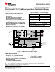
PCM5100, PCM5101, PCM5102 www.ti.com SLAS764B – MAY 2011 – REVISED SEPTEMBER 2012 2VRMS DirectPath™, 112/106/100dB Audio Stereo DAC with 32-bit, 384kHz PCM Interface Check for Samples: PCM5100, PCM5101, PCM5102 FEATURES 1 112 / 106 / 100dB Dynamic Range 112 / 106 / 100dB THD+N @ - 1dBFS –93 / –92 / –90dB Full Scale Output 2.1VRMS (GND center) Normal 8× Oversampling Digital Filter Latency: 20/fS Low Latency 8× Oversampling Digital Filter Latency: 3.
PCM5100, PCM5101, PCM5102 SLAS764B – MAY 2011 – REVISED SEPTEMBER 2012 www.ti.com This integrated circuit can be damaged by ESD. Texas Instruments recommends that all integrated circuits be handled with appropriate precautions. Failure to observe proper handling and installation procedures can cause damage. ESD damage can range from subtle performance degradation to complete device failure.
PCM5100, PCM5101, PCM5102 www.ti.com SLAS764B – MAY 2011 – REVISED SEPTEMBER 2012 This integrated circuit can be damaged by ESD. Texas Instruments recommends that all integrated circuits be handled with appropriate precautions. Failure to observe proper handling and installation procedures can cause damage. ESD damage can range from subtle performance degradation to complete device failure.
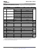
PCM5100, PCM5101, PCM5102 SLAS764B – MAY 2011 – REVISED SEPTEMBER 2012 www.ti.com ABSOLUTE MAXIMUM RATINGS over operating free-air temperature range (unless otherwise noted) VALUE Supply Voltage AVDD, CPVDD, DVDD UNIT –0.3 to 3.9 Digital Input Voltage –0.3 to 3.9 Analog Input Voltage –0.3 to 3.
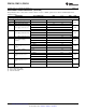
PCM5100, PCM5101, PCM5102 www.ti.com SLAS764B – MAY 2011 – REVISED SEPTEMBER 2012 ELECTRICAL CHARACTERISTICS (continued) All specifications at TA = 25°C, AVDD = CPVDD = DVDD = 3.3V, fS = 48kHz, system clock = 512 fS and 24-bit data unless otherwise noted.
PCM5100, PCM5101, PCM5102 SLAS764B – MAY 2011 – REVISED SEPTEMBER 2012 www.ti.com ELECTRICAL CHARACTERISTICS (continued) All specifications at TA = 25°C, AVDD = CPVDD = DVDD = 3.3V, fS = 48kHz, system clock = 512 fS and 24-bit data unless otherwise noted. PARAMETER TEST CONDITIONS MIN TYP MAX UNIT Power Supply Requirements DVDD Digital supply voltage 3.0 3.3 3.6 AVDD Analog supply voltage 3.0 3.3 3.6 CPVDD Charge-pump suply voltage 3.0 3.3 3.
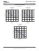
PCM5100, PCM5101, PCM5102 www.ti.com SLAS764B – MAY 2011 – REVISED SEPTEMBER 2012 TYPICAL CHARACTERISTICS All specifications at TA = 25°C, AVDD = CPVDD = DVDD = 3.3V, fS = 48kHz, system clock = 512 fS and 24-bit data unless otherwise noted. PCM5100 THD+N vs Input Level PCM5101 THD+N vs Input Level 10 -10 -10 -30 -30 THD+N [dB] THD+N [dB] 10 -50 -50 -70 -70 -90 -90 -110 -100 -110 -80 -60 -40 Input Level [dBFS] -20 -100 0 -80 -60 -40 Input Level [dBFS] Figure 2. -20 0 Figure 3.
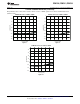
PCM5100, PCM5101, PCM5102 SLAS764B – MAY 2011 – REVISED SEPTEMBER 2012 www.ti.com TYPICAL CHARACTERISTICS (continued) All specifications at TA = 25°C, AVDD = CPVDD = DVDD = 3.3V, fS = 48kHz, system clock = 512 fS and 24-bit data unless otherwise noted.
PCM5100, PCM5101, PCM5102 www.ti.com SLAS764B – MAY 2011 – REVISED SEPTEMBER 2012 TYPICAL CHARACTERISTICS (continued) All specifications at TA = 25°C, AVDD = CPVDD = DVDD = 3.3V, fS = 48kHz, system clock = 512 fS and 24-bit data unless otherwise noted.
PCM5100, PCM5101, PCM5102 SLAS764B – MAY 2011 – REVISED SEPTEMBER 2012 www.ti.com APPLICATION INFORMATION Reset and System Clock Functions Power-On Reset Function The PCM510x includes a power-on reset function shown in Figure 11. With VDD > 2.8V, the power-on reset function is enabled. After the initialization period, the PCM510x is set to its default reset state. 3.3V 2.8V AVDD, DVDD, CPVDD Internal Reset Reset Removal Internal Reset 4 ms I2S Clocks SCK, BCK, LRCK Figure 11.
PCM5100, PCM5101, PCM5102 www.ti.com SLAS764B – MAY 2011 – REVISED SEPTEMBER 2012 System Clock Input The PCM510x requires a system clock to operate the digital interpolation filters and advanced segment DAC modulators. The system clock is applied at the SCK input (pin 12) and supports up to 50MHz. The PCM510x system-clock detection circuit automatically senses the system-clock frequency. Common audio sampling frequencies of 8kHz, 16kHz, 32kHz - 44.1kHz - 48kHz, 88.2kHz - 96kHz, 176.
PCM5100, PCM5101, PCM5102 SLAS764B – MAY 2011 – REVISED SEPTEMBER 2012 www.ti.com System Clock PLL Mode The system clock PLL mode allows designers to use a simple 3-wire I2S audio source when driving the DAC. The 3-wire source reduces the need for a high frequency SCK, making PCB layout easier, and reduces high frequency electromagnetic interference.
PCM5100, PCM5101, PCM5102 www.ti.com SLAS764B – MAY 2011 – REVISED SEPTEMBER 2012 PCM Audio Data Formats and Timing The PCM510x supports industry-standard audio data formats, including standard I2S and left-justified. Data formats are selected using the FMT (pin 16), Low for I2S, and High for Left-justified. All formats require binary 2s complement, MSB-first audio data. Figure 13 shows a detailed timing diagram for the serial audio interface. LRCK 0. 5 * DVDD (Input) tBCH t BCL tLB BCK 0.
PCM5100, PCM5101, PCM5102 SLAS764B – MAY 2011 – REVISED SEPTEMBER 2012 www.ti.com 1tS R-channel L-channel LRCK BCK Audio data word = 16-bit, BCK = 32, 48, 64fS 1 2 15 16 1 2 15 16 DATA MSB LSB MSB LSB 2 23 Audio data word = 24-bit, BCK = 48, 64fS - , 1 2 2 24 1 24 DATA MSB LSB MSB LSB Audio data word = 32-bit, BCK = 64fS 1 2 31 32 1 2 31 32 DATA MSB LSB MSB LSB Left Justified Data Format; L-channel = HIGH, R-channel = LOW Figure 14.
PCM5100, PCM5101, PCM5102 www.ti.com SLAS764B – MAY 2011 – REVISED SEPTEMBER 2012 Function Descriptions Interpolation Filter The PCM510x provides 2 types of interpolation filter. Users can select which filter to use by using the FLT pin (pin11) Table 8.
PCM5100, PCM5101, PCM5102 SLAS764B – MAY 2011 – REVISED SEPTEMBER 2012 www.ti.com 0.05 0.04 0.03 Amplitude (dB) 0.02 0.01 0.00 −0.01 −0.02 −0.03 −0.04 −0.05 0.0 0.1 0.2 0.3 Frequency (x fS) 0.4 0.5 G034 Figure 18.
PCM5100, PCM5101, PCM5102 www.ti.com SLAS764B – MAY 2011 – REVISED SEPTEMBER 2012 The Normal x4/x2/x1(bypass) Interpolation filter is programmed in 256 cycles in 1 sample time (tS) for sample rates from 8kHz to 384kHz. Table 10. Normal x4 Interpolation Filter Parameter Condition Value (Typ) Filter Gain Pass Band 0 ……. 0.45fS Filter Gain Stop Band 0.55fS ….. 7.455fS Filter Group Delay 0 Value (Max) Units ±0.02 dB –60 dB 22tS s 1.0 0.8 −20 0.6 Amplitude (FFS) Amplitude (dB) −40 −60 0.
PCM5100, PCM5101, PCM5102 SLAS764B – MAY 2011 – REVISED SEPTEMBER 2012 www.ti.com Normal x2 / x1(bypass) Interpolation filter is programmed in 256 cycles in 1 sample time (tS) for sample rates from 8kHz to 384kHz. Table 11. Normal x2 Interpolation Filter Parameter Condition Value (Typ) Filter Gain Pass Band 0 ……. 0.45fS Filter Gain Stop Band 0.55fS ….. 7.455fS Filter Group Delay 0 Value (Max) Units ±0.02 dB –60 dB 22tS s 1.0 0.8 −20 0.6 Amplitude (FFS) Amplitude (dB) −40 −60 0.4 0.
PCM5100, PCM5101, PCM5102 www.ti.com SLAS764B – MAY 2011 – REVISED SEPTEMBER 2012 The low-latency x8 / x4 / x2 / x1(bypass) Interpolation filter is programmed in 256 cycles 1 sample time (tS) for sample rates from 8kHz to 384kHz. Table 12. Low latency x8 Interpolation Filter Parameter Condition Filter Gain Pass Band 0 ……. 0.45fS Filter Gain Stop Band 0.55fS ….. 7.455fS Value (Typ) Units ±0.0001 dB –52 dB 3.5tS s Filter Group Delay 1.0 0 0.8 −20 0.
PCM5100, PCM5101, PCM5102 SLAS764B – MAY 2011 – REVISED SEPTEMBER 2012 www.ti.com Table 13. Low latency x4 Interpolation Filter Parameter Condition Filter Gain Pass Band 0 ……. 0.45fS Filter Gain Stop Band 0.55fS ….. 3.455fS Value (Typ) Units ±0.0001 dB –52 dB 3.5tS s Filter Group Delay 1.0 0 0.8 −20 0.6 Amplitude (FFS) Amplitude (dB) −40 −60 0.4 0.2 0.0 −80 −0.2 −100 −0.4 −120 0 1 2 Frequency (x fS) 3 4 −0.6 0 20 40 60 80 100 Samples G008 Figure 28.
PCM5100, PCM5101, PCM5102 www.ti.com SLAS764B – MAY 2011 – REVISED SEPTEMBER 2012 Table 14. Low latency x2 Interpolation Filter Parameter Condition Filter Gain Pass Band 0 ……. 0.45fS Filter Gain Stop Band 0.55fS ….. 1.455fS Value (Typ) Units ±0.0001 dB –52 dB 3.5tS s Filter Group Delay space 0 1.0 0.8 −20 0.6 Amplitude (FFS) Amplitude (dB) −40 −60 0.4 0.2 −80 0.0 −100 −120 −0.2 0 1 2 Frequency (x fS) 3 4 −0.4 0 10 20 30 40 50 60 Samples 70 80 90 G005 Figure 31.
PCM5100, PCM5101, PCM5102 SLAS764B – MAY 2011 – REVISED SEPTEMBER 2012 www.ti.com Zero Data Detect The PCM510x has a zero-data detect function. When the device detects continuous zero data, it enters a full analog mute condition. The PCM510x counts zero data over 1024LRCKs (21ms @ 48kHz) before setting analog mute. Power Save Mode When any kind of clock error (SCK, BCK, and LRCK) or clock halt is detected, the PCM510x enters Stand-by mode automatically.
PCM5100, PCM5101, PCM5102 www.ti.com SLAS764B – MAY 2011 – REVISED SEPTEMBER 2012 External Power Sense Undervoltage Protection mode (supported only when DVDD = 3.3V) The XSMT pin can also be used to monitor a system voltage, such as the 24VDC LCD TV backlight, or 12VDC system supply using a potential divider created with two resistors. (See Figure 35 ) • If the XSMT pin makes a transition from 1 to 0 over 6ms or more, the device will switch into external undervoltage protection mode.
PCM5100, PCM5101, PCM5102 SLAS764B – MAY 2011 – REVISED SEPTEMBER 2012 www.ti.com Recommended Powerdown Sequence With inadequate system design, the PCM510x can exhibit some pop on power down. Pops are caused by the device not having enough time to detect power loss and start the muting process. The PCM510x evaluation board avoids audible pop with an electrolytic decoupling capacitor.
PCM5100, PCM5101, PCM5102 www.ti.com SLAS764B – MAY 2011 – REVISED SEPTEMBER 2012 2. Stop I2S clocks (SCK, BCK, LRCK) 3ms before powerdown as shown below: 3.3V VDD 0V High XSMT Low 3msec High I2S Clocks SCK, BCK, LRCK Low Time Unplanned Shutdown Many systems use a low-noise regulator to provide an AVDD 3.3V supply for the DAC. The XSMT Pin can take advantage of such a feature to measure the pre-regulated output from the system SMPS to mute the DAC before the entire SMPS discharges.
PCM5100, PCM5101, PCM5102 SLAS764B – MAY 2011 – REVISED SEPTEMBER 2012 www.ti.com Typical Application Circuits PCM Audio Source Figure 38. PCM510x Standard PCM Audio Operation, 3.3V Figure 39. PCM510x PLL Operation, 3.
PCM5100, PCM5101, PCM5102 www.ti.com SLAS764B – MAY 2011 – REVISED SEPTEMBER 2012 Recommended Output Filter for the PCM510x The diagram in Figure 40 shows the recommended output filter for the PCM510x. The new PCM510x next generation current segment architecture offers excellent out of band noise, making a traditional 20kHz low pass filter a thing of the past.
PCM5100, PCM5101, PCM5102 SLAS764B – MAY 2011 – REVISED SEPTEMBER 2012 www.ti.com REVISION HISTORY Changes from Revision Initial Release (May 2011) to Revision A Page • Changed layout of first two pages ........................................................................................................................................ 1 • Deleted "Device Power Dissipation" row ..........................................................................................................................
PACKAGE OPTION ADDENDUM www.ti.
PACKAGE OPTION ADDENDUM www.ti.com 1-Feb-2013 continues to take reasonable steps to provide representative and accurate information but may not have conducted destructive testing or chemical analysis on incoming materials and chemicals. TI and TI suppliers consider certain information to be proprietary, and thus CAS numbers and other limited information may not be available for release.
IMPORTANT NOTICE Texas Instruments Incorporated and its subsidiaries (TI) reserve the right to make corrections, enhancements, improvements and other changes to its semiconductor products and services per JESD46, latest issue, and to discontinue any product or service per JESD48, latest issue. Buyers should obtain the latest relevant information before placing orders and should verify that such information is current and complete.