
Datasheet

www.ti.com
EVM Overview
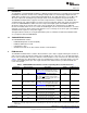
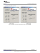
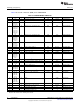
Table 1. PGA870EVM Switch Number and Corresponding Device Feature/Function
(1)
(continued)
EVM Switch Device Function Description Jumper EVM Connector
S9 B0 Gain control word LSB. A low/high signal will JP7 J8, Pin 2
decrease/increase the gain by 0.5 dB
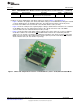
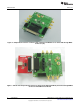
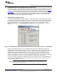
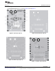
Examples of various EVM jumper and switch settings are shown in Figure 1 through Figure 3.
• Figure 1 illustrates the jumper (JP1–JP10) and switch settings for an enabled device, with gain = 20 dB
set by the EVM switches (in unlatched gain mode). The jumper block positions (JP1–JP10) on the
back side of the DB25 connector make all of the onboard switches active (S1–S9).
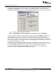
• Figure 2 shows an example of the required jumper settings to allow all device functions to be controlled
via the DB25 connector. The jumper block positions (JP1–JP10) on the back side of the DB25
connector make all of the onboard switches inactive (S1–S9).
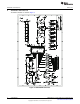
• Figure 3 shows the jumper and switch settings required for the device gain to be set from a USB port
via the GUI software. The Latch Mode, PD, and Gain Strobe functions are controlled by onboard
switches S1, S2, and S3, respectively. The jumper block positions (JP1–JP10) on the back side of the
DB25 connector make the gain-setting switches inactive (S4–S9), and the Latch Mode, PD, and Gain
Strobe switches active (S1, S2, and S3, respectively).
Figure 1. Switch and Jumper Block Positions for Enabled Device, Gain = 20 dB, Unlatched Gain Mode
3
SBOU082A–December 2009–Revised February 2010 PGA870EVM
Submit Documentation Feedback
Copyright © 2009–2010, Texas Instruments Incorporated