
Datasheet

www.ti.com
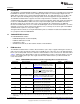
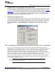
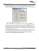
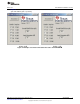
Schematic and Parts List
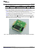
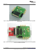
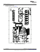
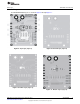
5.1 PCB Layout
The PGA870EVM PCB layers are shown in Figure 8 through Figure 11.
Figure 9. Ground Layer (Layer 2)
Figure 8. Top Layer (Layer 1)
space
Figure 10. Power Layer (Layer 3)
Figure 11. Bottom Layer (Layer 4)
9
SBOU082A–December 2009–Revised February 2010 PGA870EVM
Submit Documentation Feedback
Copyright © 2009–2010, Texas Instruments Incorporated