
User manual

SLUU186 − March 2004
7
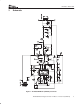
TPS40055-Based Design Converts 12-V Bus to 1.8 V at 15 A (HPA070)
4.3 UVLO Circuitry
The user programmable UVLO built into the TPS4005x provides hysteresis for transients shorter than a total
count of seven cycles. If the input voltage to the converter can be slowly rising around the minimum V
IN
range,
external hysteresis can be incorporated to prevent multiple on/off cycles during startup or shutdown. These
on/off cycles are a result of line impedance external to the EVM causing V
IN
to the module to drop when under
load, which causes the programmable UVLO threshold to be crossed repetitively.
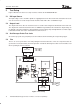
In this converter, C1 and D1 are added to form a peak detector from the lower gate drive which is only active
when the converter is operating. This provides a bias source to deliver hysteresis current from the peak detector
voltage to the lower KFF voltage of 3.5 V, enabling the designer to alter the programmable UVLO shutdown
point. The bias is not present during startup, so the circuit starts as expected from the R
KFF
calculation.
In this application, R4 is selected to provide a hysteresis current of 20% I
KFF
. R4 can be calculated from equation
(3).
R
HYS
+ R4 +
R
KFF
ǒ
V
PD
* 3.5
Ǔ
0.2
ǒ
V
IN(min)
* 3.5
Ǔ
where
D V
PD
is the voltage on the peak detector
D V
IN(min)
is the desired start voltage used in the determination of R
KFF
In a typical case, V
PD
= 8V, and R4 is found to be 247 kΩ, and a standard value of 243kΩ is selected. Testing
shows the startup voltage to be 9.2 V, and the shutdown voltage to be 8.5 V.
4.4 Inductance Value
The output inductor L1 value used in the circuit of Figure 2 was selected from equation (4).
L +
V
OUT
f I
RIPPLE
1 *
V
OUT
V
IN(min)
in which I
RIPPLE
is usually chosen to be in the range between 10% and 40% of I
OUT
. With I
RIPPLE
= 20% of
I
OUT(max)
there is a ripple current of 3 A, and the inductance value is 1.7 µH.
4.5 Input capacitor selection
Bulk input capacitor selection is based on allowable input voltage ripple and required RMS current carrying
capability. In typical buck converter applications, the converter is fed from an upstream power converter with
its own output capacitance. In this converter, ceramic capacitors capable of meeting circuit requirements are
provided onboard. For this power level, input voltage ripple of approximately 250 mV is reasonable, and the
minimum capacitance is calculated in (5).
C
IN
+
I D t
D V
+
I V
O
D V V
IN
f
S
+
15 A 1.8 V
0.25 V 10 V 300 kHz
+ 36 mF
Also consider the RMS current rating required for the input capacitors (6).
i ^ I
OUT
D
Ǹ
+ I
OUT
V
OUT
V
IN
Ǹ
+ 15
1.8
10
Ǹ
+ 6.4 A
To meet this requirement with the smallest cost and size two 22 µF, 16 V, X5R ceramic capacitors (C12, C14)
are installed on the board. In the 1812 case, the parts are able to carry approximately 4 A
RMS
each. These
capacitors function as power bypass components and should be located close to the MOSFET packages to
keep the high-frequency current flow in a small, tight loop.
(3)
(4)
(5)
(6)