
User manual

SLUU186 − March 2004
8
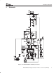
TPS40055-Based Design Converts 12-V Bus to 1.8 V at 15 A (HPA070)
4.6 Output Capacitor Selection
Selection of the output capacitor is based on many application variables, including function, cost, size, and
availability. The minimum allowable output capacitance is determined by the amount of inductor ripple current
and the allowable output ripple, as given in equation (7).
C
OUT(min)
+
I
RIPPLE
8 f V
RIPPLE
+
3A
8 300 kHz 15 mV
+ 83 mF
In this design, C
OUT(min)
is 83 µF with V
RIPPLE
=15 mV to allow for some margin. However, this only affects the
capacitive component of the ripple voltage, and the final value of capacitance is generally influenced by ESR
and transient considerations. The voltage component due to the capacitor ESR.
C
ESR
v
V
RIPPLE
I
RIPPLE
+
15 mA
3A
+ 5 mW
An additional consideration in the selection of the output inductor and capacitance value can be derived from
examining the transient voltage overshoot which can be initiated with a load step from full load to no load. By
equating the inductive energy with the capacitive energy the equation (9) can be derived:
C
O
v
L I
2
V
2
+
L
ǒ
ǒ
I
OH
Ǔ
2
*
ǒ
I
OL
Ǔ
2
Ǔ
ǒ
V
f
Ǔ
2
*
ǒ
V
i
Ǔ
2
+
1.7 mH
(
15 A
)
ǒ
(
1.9 V
)
2
*
(
1.8 V
)
2
Ǔ
+ 1034 mF
where
• I
OH
= full load current
• I
OL
= no load current
• V
f
= allowed transient voltage rise
• V
i
= initial voltage
For compactness while maintaining transient response capability, two 470-µF POSCAP capacitors (C16, C17)
are fitted in parallel. The total ESR of these capacitors is approximately 5 mΩ. An additional 47-µF, 6.3-V ceramic
capacitor C15 is placed in parallel with the POSCAPs to help suppress high frequency noise generated by the
fast current transitions as the current switches between the input and output circuits during each switching cycle.
4.7 MOSFET selection
Proper MOSFET selection is essential to optimize circuit efficiency. To operate with high current it is important
to choose a package which allows the generated heat to be removed from the package as easily as possible.
Various MOSFETs with a package similar to the SO−8 footprint are considered for this application, and devices
with reduced junction-case thermal impedance are selected.
For the upper switch Q1, a Hitachi HAT2168H MOSFET with low gate charge (typically 27 nC at 10 V) and with
an R
DS(on)
of 6 mΩ is selected to keep the switching losses to a minimum. The low-side rectifier switch Q2 was
chosen as a Hitachi HAT2167H, which has slightly more gate charge (43 nC at 10 V) but lower R
DS(on)
= 4.2
mΩ to minimize conduction losses. A schottky diode, D2, is placed across Q2 in this high current design to carry
some of the high circulating current during short circuit conditions.
(7)
(8)
(9)