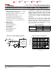
Product Folder Sample & Buy Support & Community Tools & Software Technical Documents REF3312, REF3318, REF3320, REF3325, REF3330, REF3333 SBOS392D – AUGUST 2007 – REVISED JUNE 2014 REF33xx 3.9-μA, SC70-3, SOT-23-3, and UQFN-8, 30-ppm/°C Drift Voltage Reference 1 Features 3 Description • • • • • • • • The REF33xx is a low-power, precision, low-dropout voltage reference family available in tiny SC70-3 and SOT-23-3 packages, and in a 1.5-mm × 1.5-mm UQFN-8 package.
REF3312, REF3318, REF3320, REF3325, REF3330, REF3333 SBOS392D – AUGUST 2007 – REVISED JUNE 2014 www.ti.com Table of Contents 1 2 3 4 5 6 7 Features .................................................................. Applications ........................................................... Description ............................................................. Revision History..................................................... Device Comparison ...............................................
REF3312, REF3318, REF3320, REF3325, REF3330, REF3333 www.ti.com SBOS392D – AUGUST 2007 – REVISED JUNE 2014 5 Device Comparison PRODUCT DESCRIPTION REF3312 1.25 V REF3318 1.8 V REF3320 2.048 V REF3325 2.5 V REF3330 3.0 V REF3333 3.
REF3312, REF3318, REF3320, REF3325, REF3330, REF3333 SBOS392D – AUGUST 2007 – REVISED JUNE 2014 www.ti.com 7 Specifications 7.1 Absolute Maximum Ratings over operating free-air temperature range (unless otherwise noted). (1) MIN Input voltage Voltage Output voltage Output short-circuit, ISC (2) Current Temperature (1) (2) Operating temperature –50 Junction temperature, TJ MAX UNIT 7.
REF3312, REF3318, REF3320, REF3325, REF3330, REF3333 www.ti.com SBOS392D – AUGUST 2007 – REVISED JUNE 2014 7.5 Electrical Characteristics At TA = 25°C, VIN = 5 V, and ILOAD = 0 mA (unless otherwise noted). PARAMETER TEST CONDITIONS MIN TYP MAX UNIT REF3312 (1.25 V) VOUT Output voltage 1.25 Initial accuracy –0.15% Output voltage noise V 0.15% f = 0.1 Hz to 10 Hz μVPP 35 REF3318 (1.8 V) VOUT Output voltage 1.8 Initial accuracy –0.15% Output voltage noise V 0.15% f = 0.
REF3312, REF3318, REF3320, REF3325, REF3330, REF3333 SBOS392D – AUGUST 2007 – REVISED JUNE 2014 www.ti.com Electrical Characteristics (continued) At TA = 25°C, VIN = 5 V, and ILOAD = 0 mA (unless otherwise noted). PARAMETER TEST CONDITIONS MIN TYP MAX UNIT POWER SUPPLY VS Operating voltage range IQ VOUT + 0.2 (3) Specified voltage range Current ILOAD = 0 mA 5.5 V VOUT + 0.005 5.5 V 3.9 5 μA –40°C to 85°C 4.4 6.5 μA –40°C to 125°C 4.8 8.
REF3312, REF3318, REF3320, REF3325, REF3330, REF3333 www.ti.com SBOS392D – AUGUST 2007 – REVISED JUNE 2014 7.6 Typical Characteristics Unit (%) 0 1 3 4 5 6 8 9 10 11 13 14 15 16 18 19 20 21 23 24 25 26 0 1 3 4 5 6 8 9 10 11 13 14 15 16 18 19 20 21 23 24 25 26 Unit (%) At TA = 25°C and VIN = 5 V, and REF3325 used for typical characteristic measurements (unless otherwise noted). Drift (ppm/°C) Drift (ppm/°C) 0°C to 70°C –40°C to 125°C Figure 1. Temperature Drift Figure 2. Temperature Drift 200 0.
REF3312, REF3318, REF3320, REF3325, REF3330, REF3333 SBOS392D – AUGUST 2007 – REVISED JUNE 2014 www.ti.com Typical Characteristics (continued) At TA = 25°C and VIN = 5 V, and REF3325 used for typical characteristic measurements (unless otherwise noted). 90 2.503 ILOAD = 1mA CLOAD = 1mF 80 ILOAD = 0mA 2.502 2.501 +125°C 60 Output (V) PSRR (dB) 70 50 40 30 2.500 2.499 +25°C 2.498 -40°C 20 2.497 10 2.496 2.495 0 10 100 1k 10k 100k 2.5 3.0 3.5 Frequency (Hz) 4.0 4.5 5.0 5.
REF3312, REF3318, REF3320, REF3325, REF3330, REF3333 www.ti.com SBOS392D – AUGUST 2007 – REVISED JUNE 2014 Typical Characteristics (continued) +5mA VIN -5mA -5mA ILOAD VOUT 50mV/div 10mV/div 500mV/div At TA = 25°C and VIN = 5 V, and REF3325 used for typical characteristic measurements (unless otherwise noted). VOUT Time (400ms/div) 200ms/div CLOAD = 10 μF, IOUT = 0 mA CL = 1 μF, ±5-mA Output Pulse Figure 14.
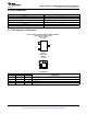
REF3312, REF3318, REF3320, REF3325, REF3330, REF3333 SBOS392D – AUGUST 2007 – REVISED JUNE 2014 www.ti.com 9 Detailed Description 9.1 Overview The REF33xx is a family of low-power, precision band-gap voltage references that are specifically designed for extremely low dropout, excellent initial voltage accuracy with a high output current. A simplified block diagram of the REF33xx is shown in the Functional Block Diagram section. Figure 17 shows the typical connections for the REF33xx.
REF3312, REF3318, REF3320, REF3325, REF3330, REF3333 www.ti.com SBOS392D – AUGUST 2007 – REVISED JUNE 2014 Feature Description (continued) 9.3.2 Low Temperature Drift The REF33xx is designed for minimal drift error, defined as the change in output voltage over temperature. The drift is calculated using the box method, as described in Equation 2: æ ö VOUTMAX - VOUTMIN 6 Drift = ç ÷ × 10 (ppm) V × Temperature Range è OUT ø (2) 9.3.
REF3312, REF3318, REF3320, REF3325, REF3330, REF3333 SBOS392D – AUGUST 2007 – REVISED JUNE 2014 www.ti.com 10 Applications and Implementation 10.1 Application Information The REF33xx is a family of low-power, precision band-gap voltage references that are specifically designed for extremely low dropout, excellent initial voltage accuracy with a high output current. The extremely small size of the SC70-3, SOT-23-3, and UQFN-8 make these references very attractive for space-constrained applications.
REF3312, REF3318, REF3320, REF3325, REF3330, REF3333 www.ti.com SBOS392D – AUGUST 2007 – REVISED JUNE 2014 Typical Applications (continued) 10.2.1.1 Design Requirements The design requirements are as follows: • Supply voltage: 3.3 V • Maximum input voltage: ±6 V • Specified input voltage: ±5 V • ADC reference voltage: 1.25 V 10.2.1.2 Detailed Design Procedure Figure 19 depicts a simplified schematic for this design showing the MSP430 ADC inputs and full input conditioning circuitry.
REF3312, REF3318, REF3320, REF3325, REF3330, REF3333 SBOS392D – AUGUST 2007 – REVISED JUNE 2014 www.ti.com Typical Applications (continued) When the ratio of R3 and R2 equals the ratio of R7 and R6, Equation 8 simplifies to Equation 10.
REF3312, REF3318, REF3320, REF3325, REF3330, REF3333 www.ti.com SBOS392D – AUGUST 2007 – REVISED JUNE 2014 The 3.3-V system supply voltage that powers the MSP430 can also supply other devices, and therefore may have regulation and noise issues. The REF3330 creates an accurate and stable 3.0 V output used by the op amp, REF3312, and other low-power analog circuitry. The REF33xx series has a drop-output voltage of VOUT + 200 mV; therefore, as long as the input supply remains above 3.
REF3312, REF3318, REF3320, REF3325, REF3330, REF3333 SBOS392D – AUGUST 2007 – REVISED JUNE 2014 f 3dB _ A1 1 R § 2S ¨ 6 © 2 www.ti.com 0.144 Hz · ¸ C2 ¹ (18) In applications that cannot tolerate such a low-frequency cutoff, and therefore a long start-up time, buffer the A1– input with another OPA317 to properly drive the ADC input with a lower-input capacitor. 10.2.1.2.
REF3312, REF3318, REF3320, REF3325, REF3330, REF3333 www.ti.com SBOS392D – AUGUST 2007 – REVISED JUNE 2014 10.2.1.3.2 AC Performance The ac transfer function for the attenuation and level-shifting circuit is shown in Figure 23. The low-frequency ac CMRR performance is measured to be 62 dB, as shown in Figure 24. 0 0 ±10 ±20 CMRR (dB) Vout (dB) ±20 ±40 ±30 ±40 ±50 ±60 ±60 ±70 ±80 ±80 1 10 100 1K 10 K Frequency (Hz) Figure 23.
REF3312, REF3318, REF3320, REF3325, REF3330, REF3333 SBOS392D – AUGUST 2007 – REVISED JUNE 2014 www.ti.com 12 Layout 12.1 Layout Guidelines For optimal performance of this design, follow standard printed circuit board (PCB) layout guidelines, including proper decoupling close to all integrated circuits and adequate power and ground connections with large copper pours. Select a PCB size with connectors that connect directly to the MSP430 LaunchPad™.
REF3312, REF3318, REF3320, REF3325, REF3330, REF3333 www.ti.com SBOS392D – AUGUST 2007 – REVISED JUNE 2014 13 Device and Documentation Support 13.1 Documentation Support 13.1.1 Related Documentation SBOS351 — OPA333 data sheet. SBOS259 — OPA363 data sheet. SBOS414 — OPA369 data sheet. SBOS333 — INA159 data sheet. 13.2 Related Links Table 2 lists quick access links. Categories include technical documents, support and community resources, tools and software, and quick access to sample or buy. Table 2.
PACKAGE OPTION ADDENDUM www.ti.
PACKAGE OPTION ADDENDUM www.ti.
PACKAGE OPTION ADDENDUM www.ti.
PACKAGE OPTION ADDENDUM www.ti.com 17-May-2014 (2) Eco Plan - The planned eco-friendly classification: Pb-Free (RoHS), Pb-Free (RoHS Exempt), or Green (RoHS & no Sb/Br) - please check http://www.ti.com/productcontent for the latest availability information and additional product content details. TBD: The Pb-Free/Green conversion plan has not been defined.
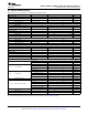
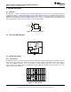
PACKAGE MATERIALS INFORMATION www.ti.com 19-Jun-2014 TAPE AND REEL INFORMATION *All dimensions are nominal Device Package Package Pins Type Drawing SPQ REF3312AIDBZR SOT-23 3000 179.0 8.4 DBZ 3 Reel Reel A0 Diameter Width (mm) (mm) W1 (mm) B0 (mm) K0 (mm) P1 (mm) W Pin1 (mm) Quadrant 3.15 2.95 1.22 4.0 8.0 Q3 REF3312AIDBZT SOT-23 DBZ 3 250 179.0 8.4 3.15 2.95 1.22 4.0 8.0 Q3 REF3312AIDCKR SC70 DCK 3 3000 179.0 8.4 2.4 2.4 1.19 4.0 8.
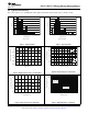
PACKAGE MATERIALS INFORMATION www.ti.com 19-Jun-2014 Device Package Package Pins Type Drawing SPQ Reel Reel A0 Diameter Width (mm) (mm) W1 (mm) B0 (mm) K0 (mm) P1 (mm) W Pin1 (mm) Quadrant REF3330AIDCKR SC70 DCK 3 3000 179.0 8.4 2.4 2.4 1.19 4.0 8.0 Q3 REF3330AIDCKT SC70 DCK 3 250 179.0 8.4 2.4 2.4 1.19 4.0 8.0 Q3 REF3330AIRSER UQFN RSE 8 5000 180.0 9.5 1.7 1.7 0.75 4.0 8.0 Q2 REF3333AIDBZR SOT-23 DBZ 3 3000 179.0 8.4 3.15 2.95 1.22 4.0 8.
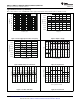
PACKAGE MATERIALS INFORMATION www.ti.com 19-Jun-2014 Device Package Type Package Drawing Pins SPQ Length (mm) Width (mm) Height (mm) REF3320AIDCKR SC70 DCK 3 3000 195.0 200.0 45.0 REF3320AIDCKT SC70 DCK 3 250 195.0 200.0 45.0 REF3325AIDBZR SOT-23 DBZ 3 3000 195.0 200.0 45.0 REF3325AIDBZT SOT-23 DBZ 3 250 195.0 200.0 45.0 REF3325AIDCKR SC70 DCK 3 3000 195.0 200.0 45.0 REF3325AIDCKT SC70 DCK 3 250 195.0 200.0 45.
IMPORTANT NOTICE Texas Instruments Incorporated and its subsidiaries (TI) reserve the right to make corrections, enhancements, improvements and other changes to its semiconductor products and services per JESD46, latest issue, and to discontinue any product or service per JESD48, latest issue. Buyers should obtain the latest relevant information before placing orders and should verify that such information is current and complete.