
Datasheet

"#$$$%
"#$$$%
SBVS001D − OCTOBER 1992 − REVISED JULY 2004
www.ti.com
8
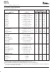
TYPICAL CHARACTERISTICS (continued)
At T
A
= +25°C, all models, unless otherwise noted.
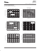
LOAD TRANSIENT RESPONSE
0.1
0
−
0.1
0.5
0
−
0.5
Load Current (A)
Output Voltage
Deviations (V)
0 20406080100
Time (
µ
s)
C
IN
=10
µ
F
C
OUT
=10
µ
F
Tantalum
V
IN
=4.25V
Preload = 0.1A
LINE TRANSIENT RESPONSE
60
40
20
0
−
20
−
40
5.25
4.25
3.25
Input Voltage (V)
Output Voltage
Deviation (mV)
0 20 40 60 80 100 120 140 160 180 200
Time (
µ
s)
C
IN
=1
µ
F
C
OUT
=10
µ
FTantalum
I
OUT
=0.1A
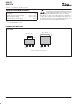
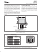
APPLICATIONS INFORMATION
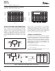
Figure 1 shows the basic hookup diagram for fixed-voltage
models. All models require an output capacitor for proper
operation, and for improving high-frequency load
regulation; a 10µF tantalum capacitor is recommended.
Aluminum electrolytic types of 50µF or greater can also be
used. A high-quality capacitor should be used to assure
that the ESR (Effective Series Resistance) is less than
0.5Ω.
REG1117
V
O
V
IN
10
µ
F
Tantalum
10
µ
F
Tantalum
++
Figure 1. Fixed-Voltage Model—Basic
Connections
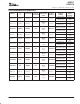
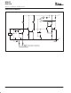
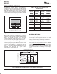
Figure 2 shows a hookup diagram for the adjustable
voltage model. Resistor values are shown for some
commonly-used output voltages. Values for other voltages
can be calculated from the equation shown in Figure 2. For
best load regulation, connect R
1
close to the output pin and
R
2
close to the ground side of the load as shown.
THERMAL CONSIDERATIONS
The REG1117 has current limit and thermal shutdown
circuits that protect it from overload. The thermal shutdown
activates at approximately T
J
= 165°C. For continuous
operation, however, the junction temperature should not
be allowed to exceed 125°C. Any tendency to activate the
thermal shutdown in normal use is an indication of an
inadequate heat sink or excessive power dissipation. The
power dissipation is equal to:
P
D
= (V
IN
– V
OUT
) I
OUT
The junction temperature can be calculated by:
T
J
= T
A
+ P
D
(q
JA
)
where T
A
is the ambient temperature, and q
JA
is the
junction-to-ambient thermal resistance.
REG1117
(Adj)
V
IN
V
O
C
2
10
µ
F
C
1
10
µ
F
C
3
(1)
10
µ
F
+
+
+
R
1
R
2
Load
32
1
NOTES: (1) C
3
optional. Improves high−frequency line rejection. (2) Resistors are standard 1% values.
V
O
= x (1.25V) + (50
µ
A) (R
2
)
R
1
R
1
+R
2
This term is negligible with
proper choice of values
−
see
table at right.
V
OUT
R
1
R
2
(
V
)(
Ω
)
(2)
(
Ω
)
(2)
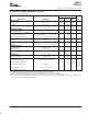
1.25 Open Short
1.5 750 147
2.1 158 107
2.85 169 215
3 137 191
3.3 115 187
5 113 340
10 113 787
Figure 2. Adjustable-Voltage Model—Basic Connections