Multipoint-Low Voltage Differential Signaling (M-LVDS) Evaluation Module User’s Guide April 2004 High Performance Analog SLLU039B
IMPORTANT NOTICE Texas Instruments Incorporated and its subsidiaries (TI) reserve the right to make corrections, modifications, enhancements, improvements, and other changes to its products and services at any time and to discontinue any product or service without notice. Customers should obtain the latest relevant information before placing orders and should verify that such information is current and complete.
EVM IMPORTANT NOTICE Texas Instruments (TI) provides the enclosed product(s) under the following conditions: This evaluation kit being sold by TI is intended for use for ENGINEERING DEVELOPMENT OR EVALUATION PURPOSES ONLY and is not considered by TI to be fit for commercial use.
EVM WARNINGS AND RESTRICTIONS It is important to operate this EVM within the supply voltage range of 3 V to 3.6 V. Exceeding the specified supply range may cause unexpected operation and/or irreversible damage to the EVM. If there are questions concerning the supply range, please contact a TI field representative prior to connecting the input power. Applying loads outside of the specified output range may result in unintended operation and/or possible permanent damage to the EVM.
Preface How to Use This Manual This document contains the following chapters: - Chapter 1—The M-LVDS Evaluation Module - Chapter 2—Test Setup - Chapter 3—Bill of Materials, Board Layout, and PCB Construction - Appendix A—Schematic Related Documentation From Texas Instruments and Others - Introduction to M-LVDS (SLLA108) - LVDS Designer’s Notes (SLLA014A). - Reducing EMI With Low Voltage Differential Signaling (SLLA030B). - Interface Circuits for TIA/EIA−644 (LVDS) (SLLA038B).
vi
Running Title—Attribute Reference Contents 1 The M-LVDS Evaluation Module . . . . . . . . . . . . . . . . . . . . . . . . . . . . . . . . . . . . . . . . . . . . . . . . . . 1.1 Overview . . . . . . . . . . . . . . . . . . . . . . . . . . . . . . . . . . . . . . . . . . . . . . . . . . . . . . . . . . . . . . . . . 1.2 M-LVDS Standard TIA/EIA−899 . . . . . . . . . . . . . . . . . . . . . . . . . . . . . . . . . . . . . . . . . . . . . . 1.3 M-LVDS EVM Kit Contents . . . . . . . . . . . . . . . . . . . . .
Running Title—Attribute Reference Figures 1−1. 1−2. 1−3 1−4 1−5 1−6 1−7 1−8 2−1 2−2 2−3 2−4 2−5 2−6 3−1 3−2 3−3 3−4 3−5 3−6 M-LVDS Unit Interval Definition . . . . . . . . . . . . . . . . . . . . . . . . . . . . . . . . . . . . . . . . . . . . . . . . . Expanded Graph of Receiver Differential Input Voltage Showing Transition Region . . . . Point-to-Point Simplex Circuit . . . . . . . . . . . . . . . . . . . . . . . . . . . . . . . . . . . . . . . . . . . . . . . . . .
Chapter 1 The M-LVDS Evaluation Module This document describes the multipoint low-voltage differential-signaling (M-LVDS) evaluation module (EVM) used to aid designers in development and analysis of this new signaling technology. The Texas Instruments SN65MLVD200A, SN65MLVD201, SN65MLVD202A, SN65MLVD203, SN65MLVD204A, SN65MLVD205A, SN65MLVD206, SN65MLVD207 series are low-voltage differential line drivers and receivers complying with the M-LVDS standard (TIA/EIA−899).
Overview 1.1 Overview The EVM comes with all the production devices in Table 1−1. The SN65MLVD201 and SN65MLVD207 are installed on the circuit board, and can easily be replaced with the other devices supplied. The M-LVDS devices evaluated with this EVM are in the SN75ALS180 and SN75176 footprint. Use of these industry standard footprints allows the designer to easily configure the parts into a simplex or half-duplex data bus. These are all TIA/EIA−899 M-LVDS standard compliant devices.
M-LVDS Standard TIA/EIA−899 The EVM has been designed with the individual driver and receiver section (SN75ALS180 footprint, U1) on one half of the board and the transceiver section (SN75176 footprint, U2) on the other half (see Figure 3−1). The EVM as delivered incorporates two 100-Ω termination resistors at each driver output, receiver input, and transceiver I/O.
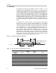
M-LVDS EVM Kit Contents Table 1−2. Receiver Input Voltage Threshold Requirements Receiver Type Low High Type-1 −2.4 V ≤ VID ≤ −0.05 V 0.05 V ≤ VID ≤ 2.4 V Type-2 −2.4 V ≤ VID ≤ 0.05 V 0.15 V ≤ VID ≤ 2.4 V Figure 1−2. Expanded Graph of Receiver Differential Input Voltage Showing Transition Region Type−1 and Type−2 Receiver Differential Input Thresholds Type 1 Type 2 2.
Configurations 1.4 Configurations The M-LVDS EVM board allows the user to construct various bus configurations. The two devices on the EVM allow for point-to-point simplex, parallel-terminated point-to-point simplex, and two-node multipoint operation. All of these modes of operation can be configured through onboard jumpers, external cabling, and different resistor combinations.
Configurations 1.4.2 Multidrop A multidrop configuration (see Figure 1−5) with two receiver nodes can be simulated with the EVM. To get additional receiver nodes on the same bus requires additional EVMs. M-LVDS controlled driver transition times and higher signal levels help to accommodate the multiple stubs and additional loads on the bus. This does not exempt good design practices, which would keep stubs short to help prevent excessive signal reflections.
Configurations Figure 1−7. Two-Node Multipoint Circuit T T U2 U1 1.4.4 EVM Operation With Separate Power Supplies The EVM has been designed with independent power planes for the two devices. The two devices can be powered with independent supplies or with a single supply. Sending and receiving data between backplanes, racks, or cabinets where separate power sources may exist can have offset ground potentials between nodes. Jumpers W7, 8, 9, and 10 tie the two separate power and ground planes together.
Recommended Equipment Figure 1−8. EVM Configuration for Including a Ground Potential Difference Voltage Between Nodes + PS1 − J13 J14 + W10 W8 W7 W9 PS2 J17 − J18 + PS3 Jumpers removed from W7, W8, W9, W10 − 1.5 Recommended Equipment - 3.3 Vdc at 0.5-A power supply or multiple power supplies (with both devices powered and enabled the board draws about 35 mA). - A 100-Ω transmission medium from the driver to the receiver, (twisted-pair cable recommended, CAT5 cable for example).
Chapter 2 Test Setup This chapter describes how to setup and use the M-LVDS EVM. Topic Page 2.1 Typical Cable Test Configurations . . . . . . . . . . . . . . . . . . . . . . . . . . . . . . 2-2 2.2 Test Results . . . . . . . . . . . . . . . . . . . . . . . . . . . . . . . . . . . . . . . . . . . . . . . . . .
Typical Cable Test Configurations 2.1 Typical Cable Test Configurations Each of the following test configurations is a transmission line consisting of a twisted-pair cable connected on the 2-pin connectors (P1, P2, or P3). Table 2−1 shows the possible configurations. In addition to the different transmission topologies, the EVM can also be configured to run off two or three separate power supplies, as described in the previous section.
Typical Cable Test Configurations 2.1.2 Point-to-Point Parallel Terminated Simplex Transmission 1) Connect a twisted-pair cable from P1 to P2. 2) Verify resistor R4 and R7 are installed. 3) Remove resistors R5 and R6. This properly terminates the transmission line at both ends. 4) Enable the driver by connecting the jumper on W2 between pin 1 and pin 2, or U1 pin 4 to VCC. 5) Enable the receiver by connecting the jumper on W1 between pin 2 and pin 3, or U1 pin 3 to GND. Figure 2−2.
Typical Cable Test Configurations Figure 2−3. Two-Node Multipoint Transmission VCC W2 Jumper Input Signal 50-Ω Cable Signal Source with 50-Ω Output 4 J2 5 R3 49.
Test Results 2.2 Test Results The test configurations described in Section 2.1 were used to simulate pointto-point simplex, parallel-terminated point-to-point simplex, and two-node multipoint. The test results are shown in the following figures. A Tektronix HFS9003 was used to generate input signals, and a Tektronix TDS784D was used to collect the output data. The EVM was populated with a SN65MLVD207D and SN65MLVD201D for U1 and U2 respectively.
Test Results signal on TP1, R2 is shorted. Type-2 behavior is again observed on the SN65MLVD207 receiver output. Trace three shows the differential voltage on the bus. Note that the bus voltages are nominal M-LVDS levels of 1.1 VPP due to the lower load seen by the current driver. Figure 2−5.
Chapter 3 Bill of Materials, Board Layout, and PCB Construction This chapter contains the bill of materials, board layout of the M-LVDS, and describes the printed-circuit board. Topic Page 2.1 Bill of Materials . . . . . . . . . . . . . . . . . . . . . . . . . . . . . . . . . . . . . . . . . . . . . . . 3-2 3.2 Board Layout . . . . . . . . . . . . . . . . . . . . . . . . . . . . . . . . . . . . . . . . . . . . . . . . . 3-3 3.3 PCB Construction . . . . . . . . . . . . . . . . . . . . . . . . . . .
Bill of Materials 3.1 Bill of Materials Table 3−1. M-LVDS EVM Bill of Materials Item No. Qty. 1 2 C1, C2 Capacitor, SMT1206, 50 V, 10%, 0.
Board Layout 3.2 Board Layout Figure 3−1. Assembly Drawing J8 J7 J18 R12 TP4W4 W3 VCC01 J15 GND01 VCC01 R14 J16 GND01 TP3 VCC01 GND01 VCC01 J14 W10GND GND VCC W8 J1 J2 J13 VCC R1 W2 W1 TP1 VCC TP2 R2 VCC J12 R4 P1 R5 GND R8 R10 R3 R13 MADE IN U2 U.S.A. TEXAS INSTRUMENTS U1 A/W NO. # 6424409B R15 R7 PWA. EVM. P3 P2 SN65MLVD SERIAL NO.
Board Layout The second layer of the EVM has the separate ground planes. These are the reference planes for the controlled impedance traces on the top layer. Figure 3−3.
Board Layout The bottom layer of the EVM contains bulk and decoupling capacitors to be placed close to the power and ground pins on the device. Figure 3−5.
PCB Construction 3.3 PCB Construction Information in this section was obtained from the following source: - Electromagnetic Compatibility Printed Circuit Board and Electronic Module Design, VEC workshop, Violette Engineering Corporation. Characteristic impedance is the ratio of voltage to current in a transmission line wave traveling in one direction. This characteristic impedance is the value that is matched with our termination resistors so as to reduce reflections.
PCB Construction Figure 3−6. Trace Configurations in Printed-Circuit Boards W t W Board Material h MICROSTRIP S W t STRIPLINE Stripline construction is the preferred configuration for differential signaling. This configuration reduces radiated emissions from circuit board traces due to better control of the lines of flux. The additional ground plane also allows for better control of impedance on the traces.
PCB Construction Table 3−2 shows the layer stack up of the EVM with the defined trace widths for the controlled impedance etch runs using microstrip construction. Table 3−2. EVM Layer Stack Up Differential Model Material Type: FR 406 Layer No. Layer Type Thickness (mils) Copper Weight Line Width (mils) Spacing (mils) Impedance (Ω) Line Width (mils) Impedance (Ω) 1 Signal 0.0006 0.5 oz (start) 0.027 0.230 100 0.0420 50 0.027 0.230 100 0.0420 50 PREPREG 0.025 2 Plane CORE 0.
Appendix A Schematic This Appendix contains the EVM schematic.
1 2 3 4 5 6 V CC R2 453 W1 ReceiverO utput D W2 C1 0.01uF J1 R1* 49.9 D R8* 0.0 TP1 J3* ReceiverInput+ U1 1 2 ReceiverEnable 3 D riverEnable 4 5 D riverInput J2 5 R3 49.9 TP2 7 NC V cc R V cc RE A DE B D Z GND Y GND NC 14 R4 100 13 P1 R5 100 12 R9* 0.0 J4* 11 RecieverInputJ5* 10 D riverO utputR10* 0.0 9 8 R7 100 SN 65M LV D 202,203,205,O R 207 P2 R6 100 C R11* 0.0 C J6* GND D riverO utput+ V CC01 W3 R13 453 W4 C2 0.