
Car Stereo System - Car Radio Digital Signal Processor User Manual

www.ti.com
32K bytes
32K bytes
64K bytes
128K bytes
1840K bytes
L2 memory
0080 0000h
009C 0000h
009E 0000h
009F 0000h
009F 8000h
00A0 0000h
7/8
SRAM
4-way
cache
4-way
cache
SRAM
15/16
4-way
31/32
SRAM
4-way
SRAM
63/64
All
SRAM
000 001 010 011 111
Block base
address
L2 mode bits
cache
SM320C6455-EP
FIXED-POINT DIGITAL SIGNAL PROCESSOR
SPRS462B – SEPTEMBER 2007 – REVISED JANUARY 2008
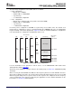
The L2 memory configuration for the C6455 device is as follows:
• Port 0 configuration:
– Memory size is 2096KB
– Starting address is 0080 0000h
– 2-cycle latency
– 4 × 128 bit bank configuration
• Port 1 configuration:
– Memory size is 32K bytes (this corresponds to the internal ROM)
– Starting address is 0010 0000h
– 1-cycle latency
– 1 × 256 bit bank configuration
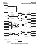
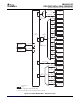
L2 memory can be configured as all SRAM or as part 4-way set-associative cache. The amount of L2
memory that is configured as cache is controlled through the L2MODE field of the L2 Configuration
Register (L2CFG) of the C64x+ Megamodule. Figure 5-4 shows the available SRAM/cache configurations
for L2. By default, L2 is configured as all SRAM after device reset.
Figure 5-4. C6455 L2 Memory Configurations
For more information on the operation L1 and L2 caches, see the TMS320C64x+ DSP Cache User's
Guide (literature number SPRU862 ).
All memory on the C6455 has a unique location in the memory map (see Table 2-2 , C6455 Memory Map
Summary).
When accessing the internal ROM of the DSP, the CPU frequency must be less than 750 MHz. Therefore,
when using a software boot mode, care must be taken such that the CPU frequency does not exceed 750
MHz at any point during the boot sequence. After the boot sequence has completed, the CPU frequency
can be programmed to the frequency required by the application. For more detailed information on the
boot modes, see Section 2.4 , Boot Sequence.
Submit Documentation Feedback C64x+ Megamodule 89