
Datasheet


Table Of Contents
1
FEATURES
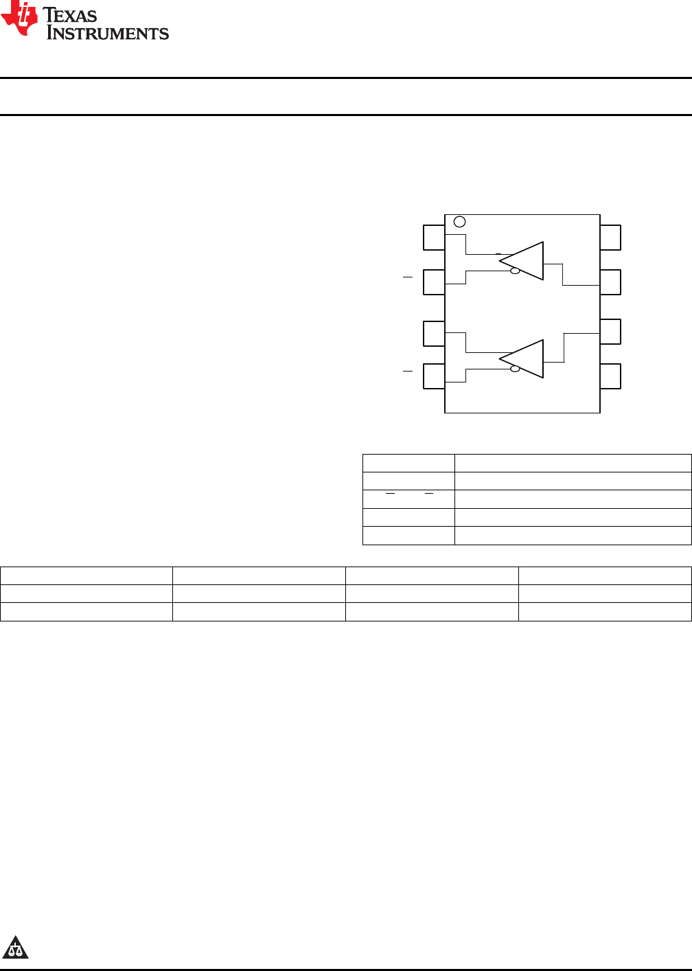
PIN ASSIGNMENT
APPLICATIONS
DESCRIPTION
1 8
2 7
3
6
4 5
V
CC
GND
Q
0
Q
0
Q
1
Q
1
D
0
D
1
SN65ELT22
www.ti.com
............................................................................................................................................................................................ SLLS924 – DECEMBER 2008
5-V Dual TTL-to-Differential PECL Translator
• 1.1-ns (max) Propagation Delay
• Operating Range: V
CC
= 4.2V to 5.7V with
D or DGK PACKAGE
GND = 0 V
(TOP VIEW)
• < 50-ps (typ) Output-to-Output Skew
• Built-In Temperature Compensation
• Drop-In Compatible to the MC10ELT22,
MC100ELT22
• Data and Clock Transmission Over Backplane
• Signaling Level Conversion for Clock or Data
The SN65ELT22 is a dual TTL-to-differential PECL
translator. It operates on +5-V supply and ground
only. The output is undetermined when the inputs are
Table 1. Pin Descriptions
left floating. The low output skew makes the device
an ideal solution for clock or data signal translation.
PIN FUNCTION
The SN65ELT22 is housed in an industry standard
D
0
, D
1
TTL inputs
SOIC-8 package and is also available in an optional
Q
0
, Q
0
, Q
1
, Q
1
PECL outputs
TSSOP-8 package.
V
CC
Positive supply
GND Ground
ORDERING INFORMATION
(1)
PART NUMBER PART MARKING PACKAGE LEAD FINISH
SN65ELT22D SN65ELT22 SOIC NiPdAu
SN65ELT22DGK SN65ELT22 SOIC-TSSOP NiPdAu
(1) Leaded device options are not initially available; contact a sales representative for further details
1
Please be aware that an important notice concerning availability, standard warranty, and use in critical applications of Texas
Instruments semiconductor products and disclaimers thereto appears at the end of this data sheet.
PRODUCTION DATA information is current as of publication date.
Copyright © 2008, Texas Instruments Incorporated
Products conform to specifications per the terms of the Texas
Instruments standard warranty. Production processing does not
necessarily include testing of all parameters.