
Datasheet


Table Of Contents
- FEATURES
- APPLICATIONS
- DESCRIPTION
- ABSOLUTE MAXIMUM RATINGS
- POWER DISSIPATION RATINGS
- THERMAL CHARACTERISTICS
- KEY ATTRIBUTES
- LVTTL OUTPUT DC CHARACTERISTICS (VCC = 3.3 V; GND = 0 V, TA = -40C to 85C)
- LVPECL INPUT DC CHARACTERISTICS (VCC = 3.3 V; GND = 0.0 V)
- AC CHARACTERISTICS (VCC = 3.0 V to 3.6 V; GND = 0.0 V)
- REVISION HISTORY
1
8
2
7
3
6
4
5
D0
Q0
Q1
V
CC
D0
D1
GND
D1
LVPECL
LVTTL
+
+
+
+
+
SN65EPT23
www.ti.com
SLLS969A – NOVEMBER 2009– REVISED JANUARY 2011
3.3V ECL Differential LVPECL/LVDS to LVTTL/LVCMOS Translator
Check for Samples: SN65EPT23
1
FEATURES
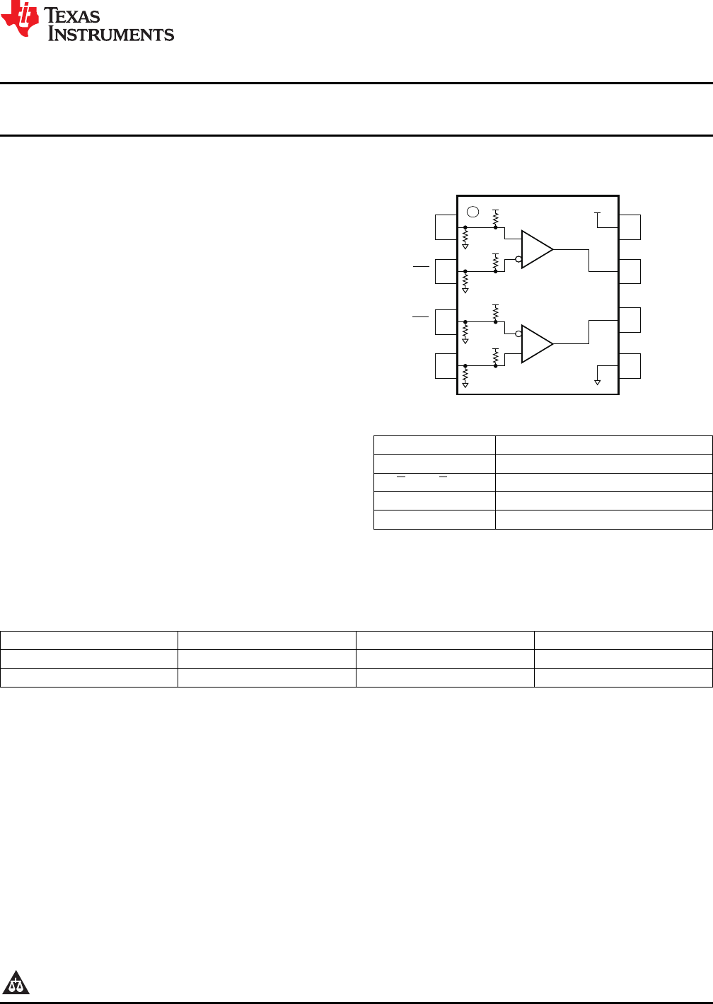
PINOUT ASSIGNMENT
• Dual 3.3 V Differential LVPECL/LVDS to
LVTTL/LVCMOS Buffer Translator
• 24 mA LVTTL Ouputs
• Operating Range
– V
CC
= 3.0 V to 3.6 V
– GND = 0 V
• Support for Clock Frequencies > 300 MHz
• 2.0 ns Typical Propagation Delay
• Built-in Temperature Compensation
• Drop in Compatible to MC100EPT23
APPLICATIONS
• Data and Clock Transmission Over Backplane
Table 1. Pin Description
• Signaling Level Conversion for Clock or Data
PIN FUNCTION
Q
0
, Q
1
LVTTL/LVCMOS Outputs
DESCRIPTION
D
0
, D
0
, D
1
, D
1
Differential LVPECL/LVDS/CML Inputs
The SN65EPT23 is a low power dual LVPECL/LVDS
V
CC
Positive Supply
to LVTTL/LVCMOS translator device. The device
includes circuitry to maintain inputs at Vcc/2 when left GND Ground
open. The SN65EPT23 is housed in an industry
standard SOIC-8 package and is also available in
TSSOP-8 option.
spacer
ORDERING INFORMATION
(1)
PART NUMBER PART MARKING PACKAGE LEAD FINISH
SN65EPT23D/DR EPT23 SOIC NiPdAu
SN65EPT23DGK/DGKR SSTI MSOP NiPdAu
(1) Leaded device option not initially available; contact TI sales representative for further information.
1
Please be aware that an important notice concerning availability, standard warranty, and use in critical applications of Texas
Instruments semiconductor products and disclaimers thereto appears at the end of this data sheet.
PRODUCTION DATA information is current as of publication date.
© 2009–2011, Texas Instruments Incorporated
Products conform to specifications per the terms of the Texas
Instruments standard warranty. Production processing does not
necessarily include testing of all parameters.