
Digital Input Serializer User's Guide


1 Introduction
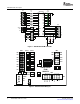
2 EVM Schematic and Layout
User's Guide
SLAU245 – March 2008
SN65HVS880 EVM User's Guide
The SN65HVS880 evaluation module (EVM) supports the parametric evaluation of the SN65HVS880
digital input serializer. It is intended to be used in conjunction with the SN65HVS880 data sheet,
(SLAS252 ).
Note: this EVM is not intended for electromagnetic compatibility (EMC) tests.
Figure 1 shows the board circuit schematic, and Figure 2 shows the board layout top view. The board
includes a terminal block, TB1, and four connectors, JMP1 to 4.
TB1 receives the board supply of 24V nominal. V24 supplies the SN65HVS880 device, and VFIELD
provides the supply for sensor switches.
Upon the application of V24, the blue Chip-Okay LED (CHOK) indicates proper board function. At the
same time, the red LED indicates 5V availability at the regulator output 5VOP.
JMP1 provides the field inputs IN0:IN7 for field voltages of 24V nominal. They can be applied via:
a. an external supply in series to a sensor switch connected to a field input,
b. or a sensor switch connected between and input and VFIELD,
c. or a direct connection between an input and VFIELD.
In all three cases, a 24V level represents the ON-status of a sensor switch, which is indicated by the
corresponding LEDs D0:D7.
JMP2 provides access to the control and data lines of the internal serializer. To operate the serializer, CE
must be connected either to ground or to CLK.
Upon an active-low load pulse, (a high-to-low-to-high transition) at LD, the status information of the field
inputs is latched into the serializer. Applying eight consecutive clock cycles at CLK, shifts out the serializer
data at SOP with each rising edge of the clock.
Cascading of multiple boards is also possible by connecting the SOP output of a leading device with the
SIP input of a following device.
JMP3 allows the selection of three different debounce times and 3 different current limits.
Debounce default is 3ms, and does not require any connection between the DB inputs to ground.
Otherwise, for zero debounce time connect DB1 to ground, and for 1ms debounce time connect DB0 to
ground.
Note: the open DB inputs are internally pulled high and will not float.
Setting a specific current limit requires a connection between the R
LIM
output and one of the resistors, R
LIM
1:3. For a current limit of 3.6mA connect R
LIM
to 24.9k Ω , for 3mA to 30.1k Ω , and for 2.5mA to 36.1k Ω .
JMP4 allows to connect VFIELD to V24, thus driving the board with only one supply.
For detailed information on device functionality and system design recommendations, see the
SN65HVS880 data sheet.
SLAU245 – March 2008 SN65HVS880 EVM User's Guide 1
Submit Documentation Feedback