
Datasheet


SN54ABT16240A, SN74ABT16240A
16-BIT BUFFERS/DRIVERS
WITH 3-STATE OUTPUTS
SCBS095G – DECEMBER 1991 – REVISED OCTOBER 1998
4
POST OFFICE BOX 655303 • DALLAS, TEXAS 75265
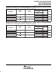
recommended operating conditions (see Note 3)
SN54ABT16240A SN74ABT16240A
UNIT
MIN MAX MIN MAX
UNIT
V
CC
Supply voltage 4.5 5.5 4.5 5.5 V
V
IH
High-level input voltage 2 2 V
V
IL
Low-level input voltage 0.8 0.8 V
V
I
Input voltage 0 V
CC
0 V
CC
V
I
OH
High-level output current –24 –32 mA
I
OL
Low-level output current 48 64 mA
∆t/∆v Input transition rise or fall rate Outputs enabled 10 10 ns/V
T
A
Operating free-air temperature –55 125 –40 85 °C
NOTE 3: All unused inputs of the device must be held at V
CC
or GND to ensure proper device operation. Refer to the TI application report,
Implications of Slow or Floating CMOS Inputs
, literature number SCBA004.
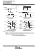
electrical characteristics over recommended operating free-air temperature range (unless
otherwise noted)
PARAMETER
TEST CONDITIONS
T
A
= 25°C SN54ABT16240A SN74ABT16240A
UNIT
PARAMETER
TEST
CONDITIONS
MIN TYP
†
MAX MIN MAX MIN MAX
UNIT
V
IK
V
CC
= 4.5 V, I
I
= –18 mA –1.2 –1.2 –1.2 V
V
CC
= 4.5 V, I
OH
= –3 mA 2.5 2.5 2.5
V
OH
V
CC
= 5 V, I
OH
= –3 mA 3 3 3
V
V
OH
V
CC
=45V
I
OH
= –24 mA 2 2
V
V
CC
=
4
.
5
V
I
OH
= –32 mA 2* 2
V
OL
V
CC
=45V
I
OL
= 48 mA 0.55 0.55
V
V
OL
V
CC
=
4
.
5
V
I
OL
= 64 mA 0.55* 0.55
V
V
hys
100 mV
I
I
V
CC
= 5.5 V, V
I
= V
CC
or GND ±1 ±1 ±1 µA
I
OZH
V
CC
= 5.5 V, V
O
= 2.7 V 10 10 10 µA
I
OZL
V
CC
= 5.5 V, V
O
= 0.5 V –10 –10 –10 µA
I
off
V
CC
= 0, V
I
or V
O
≤ 4.5 V ±100 ±100 µA
I
CEX
V
CC
= 5.5 V,
V
O
= 5.5 V
Outputs high 50 50 50 µA
I
O
‡
V
CC
= 5.5 V, V
O
= 2.5 V –50 –100 –180 –50 –180 –50 –180 mA
V
CC
=
5.5 V,
Outputs high 3 3 3
I
CC
V
CC
=
5
.
5
V
,
I
O
= 0,
Outputs low 34 34 34
mA
V
I
= V
CC
or GND
Outputs disabled 3 3 3
§
Data
V
CC
= 5.5 V,
One input at 3.4 V,
Outputs enabled 1 1.5 1
∆I
CC
§
inputs
,
Other inputs at
V
CC
or GND
Outputs disabled 0.05 1 0.05
mA
Control
inputs
V
CC
= 5.5 V, One input at 3.4 V,
Other inputs at V
CC
or GND
1.5 1.5 1.5
C
i
V
I
= 2.5 V or 0.5 V 3.5 pF
C
o
V
O
= 2.5 V or 0.5 V 7.5 pF
* On products compliant to MIL-PRF-38535, this parameter does not apply.
†
All typical values are at V
CC
= 5 V.
‡
Not more than one output should be tested at a time, and the duration of the test should not exceed one second.
§
This is the increase in supply current for each input that is at the specified TTL voltage level rather than V
CC
or GND.