
Datasheet


SN54ABT16240A, SN74ABT16240A
16-BIT BUFFERS/DRIVERS
WITH 3-STATE OUTPUTS
SCBS095G – DECEMBER 1991 – REVISED OCTOBER 1998
6
POST OFFICE BOX 655303 • DALLAS, TEXAS 75265
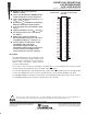
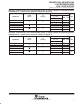
PARAMETER MEASUREMENT INFORMATION
1.5 V
t
h
t
su
From Output
Under Test
C
L
= 50 pF
(see Note A)
LOAD CIRCUIT
S1
7 V
Open
GND
500 Ω
500 Ω
Data Input
Timing Input
1.5 V
3 V
0 V
1.5 V 1.5 V
3 V
0 V
3 V
0 V
1.5 V
t
w
Input
VOLTAGE WAVEFORMS
SETUP AND HOLD TIMES
VOLTAGE WAVEFORMS
PROPAGATION DELAY TIMES
INVERTING AND NONINVERTING OUTPUTS
VOLTAGE WAVEFORMS
PULSE DURATION
t
PLH
t
PHL
t
PHL
t
PLH
V
OH
V
OH
V
OL
V
OL
1.5 V 1.5 V
3 V
0 V
1.5 V1.5 V
Input
1.5 V
Output
Control
Output
Waveform 1
S1 at 7 V
(see Note B)
Output
Waveform 2
S1 at Open
(see Note B)
V
OL
V
OH
t
PZL
t
PZH
t
PLZ
t
PHZ
1.5 V1.5 V
3.5 V
0 V
1.5 V
V
OL
+ 0.3 V
1.5 V
V
OH
– 0.3 V
≈ 0 V
3 V
VOLTAGE WAVEFORMS
ENABLE AND DISABLE TIMES
LOW- AND HIGH-LEVEL ENABLING
Output
Output
t
PLH
/t
PHL
t
PLZ
/t
PZL
t
PHZ
/t
PZH
Open
7 V
Open
TEST S1
Output
Control
NOTES: A. C
L
includes probe and jig capacitance.
B. Waveform 1 is for an output with internal conditions such that the output is low except when disabled by the output control.
Waveform 2 is for an output with internal conditions such that the output is high except when disabled by the output control.
C. All input pulses are supplied by generators having the following characteristics: PRR ≤ 10 MHz, Z
O
= 50 Ω, t
r
≤ 2.5 ns, t
f
≤ 2.5 ns.
D. The outputs are measured one at a time with one transition per measurement.
1.5 V
Figure 1. Load Circuit and Voltage Waveforms