
Datasheet


SN54ABTR2245, SN74ABTR2245
OCTAL TRANSCEIVERS AND LINE/MEMORY DRIVERS
WITH 3-STATE OUTPUTS
SCBS680A – MARCH 1997 – REVISED MAY 1997
1
POST OFFICE BOX 655303 • DALLAS, TEXAS 75265
Outputs Have Equivalent 25-Ω Series
Resistors, So No External Resistors Are
Required
State-of-the-Art
EPIC-
ΙΙ
B
BiCMOS Design
Significantly Reduces Power Dissipation
High-Impedance State During Power Up
and Power Down
Latch-Up Performance Exceeds 500 mA Per
JEDEC Standard JESD-17
ESD Protection Exceeds 2000 V Per
MIL-STD-833, Method 3015; Exceeds 200 V
Using Machine Model (C = 200 pF, R = 0)
Typical V
OLP
(Output Ground Bounce) < 1 V
at V
CC
= 5 V, T
A
= 25°C
Package Options Include Plastic
Small-Outline (DW), Shrink Small-Outline
(DB), Thin Shrink Small-Outline (PW), and
Thin Very Small-Outline (DGV) Packages,
Ceramic Chip Carriers (FK), and Plastic (N)
and Ceramic (J) DIPs
description
These octal transceivers and line drivers are
designed for asynchronous communication
between data buses. The devices transmit data
from the A bus to the B bus or from the B bus to
the A bus, depending on the logic level at the
direction-control (DIR) input. The output-enable
(OE
) input can be used to disable the device so
the buses are effectively isolated.
Both the A-port and B-port outputs, which are designed to sink up to 12 mA, include equivalent 25-Ω series
resistors to reduce overshoot and undershoot.
When V
CC
is between 0 and 2.1 V, the device is in the high-impedance state during power up or power down.
However, to ensure the high-impedance state above 2.1 V, OE
should be tied to V
CC
through a pullup resistor;
the minimum value of the resistor is determined by the current-sinking capability of the driver.
The SN54ABTR2245 is characterized for operation over the full military temperature range of –55°C to 125°C.
The SN74ABTR2245 is characterized for operation from –40°C to 85°C.
FUNCTION TABLE
INPUTS
OPERATION
OE DIR
OPERATION
L L B data to A bus
L H A data to B bus
H X Isolation
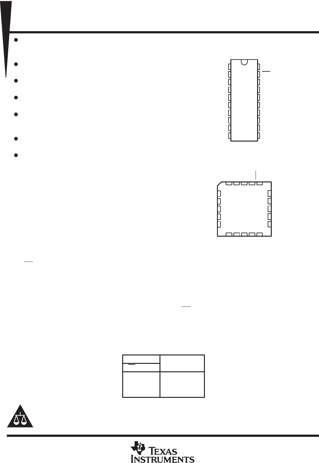
SN54ABTR2245 ...J PACKAGE
SN74ABTR2245 . . . DB, DGV, DW, N, OR PW PACKAGE
(TOP VIEW)
3212019
9
10 11 12 13
4
5
6
7
8
18
17
16
15
14
B1
B2
B3
B4
B5
A3
A4
A5
A6
A7
A2
A1
DIR
B7
B6 OE
A8
GND
B8
V
CC
SN54ABTR2245 . . . FK PACKAGE
(TOP VIEW)
1
2
3
4
5
6
7
8
9
10
20
19
18
17
16
15
14
13
12
11
DIR
A1
A2
A3
A4
A5
A6
A7
A8
GND
V
CC
OE
B1
B2
B3
B4
B5
B6
B7
B8
EPIC-ΙΙB is a trademark of Texas Instruments Incorporated.
Copyright 1997, Texas Instruments Incorporated
UNLESS OTHERWISE NOTED this document contains PRODUCTION
DATA information current as of publication date. Products conform to
specifications per the terms of Texas Instruments standard warranty.
Production processing does not necessarily include testing of all
parameters.
Please be aware that an important notice concerning availability, standard warranty, and use in critical applications of
Texas Instruments semiconductor products and disclaimers thereto appears at the end of this data sheet.