
Datasheet


SN54AHC02, SN74AHC02
QUADRUPLE 2-INPUT POSITIVE-NOR GATES
SCLS254K− DECEMBER 1995 − REVISED JULY 2003
2
POST OFFICE BOX 655303 • DALLAS, TEXAS 75265
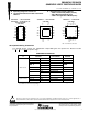
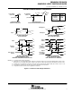
FUNCTION TABLE
(each gate)
INPUTS
OUTPUT
A B
OUTPUT
Y
H X L
X HL
L L H
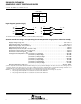
logic diagram (positive logic)
2
1A
3
1B
1Y
1
8
3A
9
3B
3Y
10
5
2A
6
2B
2Y
4
11
4A
12
4B
4Y
13
Pin numbers shown are for the D, DB, DGV, J, N, NS, PW, RGY, and W packages.
absolute maximum ratings over operating free-air temperature range (unless otherwise noted)
†
Supply voltage range, V
CC
−0.5 V to 7 V. . . . . . . . . . . . . . . . . . . . . . . . . . . . . . . . . . . . . . . . . . . . . . . . . . . . . . . . . .
Input voltage range, V
I
(see Note 1) −0.5 V to 7 V. . . . . . . . . . . . . . . . . . . . . . . . . . . . . . . . . . . . . . . . . . . . . . . . . .
Output voltage range, V
O
(see Note 1) −0.5 V to V
CC
+ 0.5 V. . . . . . . . . . . . . . . . . . . . . . . . . . . . . . . . . . . . . . . . .
Input clamp current, I
IK
(V
I
< 0) −20 mA. . . . . . . . . . . . . . . . . . . . . . . . . . . . . . . . . . . . . . . . . . . . . . . . . . . . . . . . . . .
Output clamp current, I
OK
(V
O
< 0 or V
O
> V
CC
) ±20 mA. . . . . . . . . . . . . . . . . . . . . . . . . . . . . . . . . . . . . . . . . . . . .
Continuous output current, I
O
(V
O
= 0 to V
CC
) ±25 mA. . . . . . . . . . . . . . . . . . . . . . . . . . . . . . . . . . . . . . . . . . . . . .
Continuous current through V
CC
or GND ±50 mA. . . . . . . . . . . . . . . . . . . . . . . . . . . . . . . . . . . . . . . . . . . . . . . . . . .
Package thermal impedance, θ
JA
(see Note 2): D package 86°C/W. . . . . . . . . . . . . . . . . . . . . . . . . . . . . . . . . . .
(see Note 2): DB package 96°C/W. . . . . . . . . . . . . . . . . . . . . . . . . . . . . . . . .
(see Note 2): DGV package 127°C/W. . . . . . . . . . . . . . . . . . . . . . . . . . . . . . .
(see Note 2): N package 80°C/W. . . . . . . . . . . . . . . . . . . . . . . . . . . . . . . . . . .
(see Note 2): NS package 76°C/W. . . . . . . . . . . . . . . . . . . . . . . . . . . . . . . . .
(see Note 2): PW package 113°C/W. . . . . . . . . . . . . . . . . . . . . . . . . . . . . . . .
(see Note 3): RGY package 47°C/W. . . . . . . . . . . . . . . . . . . . . . . . . . . . . . . .
Storage temperature range, T
stg
−65°C to 150°C. . . . . . . . . . . . . . . . . . . . . . . . . . . . . . . . . . . . . . . . . . . . . . . . . . .
†
Stresses beyond those listed under “absolute maximum ratings” may cause permanent damage to the device. These are stress ratings only, and
functional operation of the device at these or any other conditions beyond those indicated under “recommended operating conditions” is not
implied. Exposure to absolute-maximum-rated conditions for extended periods may affect device reliability.
NOTES: 1. The input and output voltage ratings may be exceeded if the input and output current ratings are observed.
2. The package thermal impedance is calculated in accordance with JESD 51-7.
3. The package thermal impedance is calculated in accordance with JESD 51-5.