
Datasheet


1
2
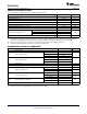
4
A
B
Y
3
2
4
51
A V
CC
Y
B
GND
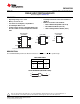
DBV PACKAGE
(TOP VIEW)
DCK PACKAGE
(TOP VIEW)
3
2
4
51
A V
CC
Y
B
GND
3
2
4
51
A V
CC
Y
B
GND
DRL PACKAGE
(TOP VIEW)
SN74AHC1G00
www.ti.com
SCLS313N –MARCH 1996–REVISED MAY 2013
SINGLE 2-INPUT POSITIVE-NAND GATE
Check for Samples: SN74AHC1G00
1
FEATURES
• Operating Range 2-V to 5.5-V • Latch-Up Performance Exceeds 250 mA Per
JESD 17
• Max t
pd
of 6.5ns at 5-V
• ESD Protection Exceeds JESD 22
• Low Power Consumption, 10-μA Max I
CC
– 2000-V Human-Body Model (A114-A)
• ±8-mA Output Drive at 5-V
– 200-V Machine Model (A115-A)
• Schmitt Trigger Action at All Inputs Makes the
Circuit Tolerant for Slower Input Rise and Fall – 1000-V Charged-Device Model (C101)
Time
See mechanical drawings for dimensions.
DESCRIPTION
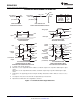
The SN74AHC1G00 performs the Boolean function Y = A • B or Y = A + B in positive logic.
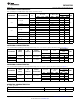
FUNCTION TABLE
INPUTS OUTPUT
A B Y
H H L
L X H
X L H
LOGIC DIAGRAM (POSITIVE LOGIC)
1
Please be aware that an important notice concerning availability, standard warranty, and use in critical applications of
Texas Instruments semiconductor products and disclaimers thereto appears at the end of this data sheet.
PRODUCTION DATA information is current as of publication date.
Copyright © 1996–2013, Texas Instruments Incorporated
Products conform to specifications per the terms of the Texas
Instruments standard warranty. Production processing does not
necessarily include testing of all parameters.