
Datasheet


SCLS317N − MARCH 1996 − REVISED JUNE 2005
1
POST OFFICE BOX 655303 • DALLAS, TEXAS 75265
D Operating Range of 2 V to 5.5 V
D Max t
pd
of 6.5 ns at 5 V
D Low Power Consumption, 10-µA Max I
CC
D ±8-mA Output Drive at 5 V
D Schmitt Trigger Action at All Inputs Makes
the Circuit Tolerant for Slower Input Rise
and Fall Time
D Latch-Up Performance Exceeds 250 mA Per
JESD 17
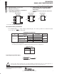
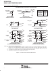
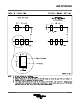
3
2
4
51
AV
CC
Y
B
GND
DBV PACKAGE
(TOP VIEW)
DCK PACKAGE
(TOP VIEW)
3
2
4
51
AV
CC
Y
B
GND
3
2
4
51
AV
CC
Y
B
GND
DRL PACKAGE
(TOP VIEW)
See mechanical drawings for dimensions.
description/ordering information
The SN74AHC1G32 is a single 2-input positive-OR gate. The device performs the Boolean function
Y + A ) BorY+ A
• B in positive logic.
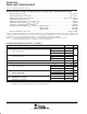
ORDERING INFORMATION
T
A
PACKAGE
†
ORDERABLE
PART NUMBER
TOP-SIDE
MARKING
‡
SOT (SOT-23) − DBV
Reel of 3000 SN74AHC1G32DBVR
A32_
SOT (SOT-23) − DBV
Reel of 250 SN74AHC1G32DBVT
A32_
−40°C to 85°C
SOT (SC-70) − DCK
Reel of 3000 SN74AHC1G32DCKR
AG_
−40 C to 85 C
SOT (SC-70) − DCK
Reel of 250 SN74AHC1G32DCKT
AG_
SOT (SOT-553) – DRL Reel of 4000 SN74AHC1G32DRLR AG_
†
Package drawings, standard packing quantities, thermal data, symbolization, and PCB design guidelines are
available at www.ti.com/sc/package.
‡
The actual top-side marking has one additional character that designates the assembly/test site.
FUNCTION TABLE
INPUTS
OUTPUT
A B
OUTPUT
Y
H X H
X HH
L L L
logic diagram (positive logic)
1
2
4
A
B
Y
Copyright 2005, Texas Instruments Incorporated
!"# $"%&! '#(
'"! ! $#!! $# )# # #* "#
'' +,( '"! $!#- '# #!#&, !&"'#
#- && $##(
Please be aware that an important notice concerning availability, standard warranty, and use in critical applications of
Texas Instruments semiconductor products and disclaimers thereto appears at the end of this data sheet.