
Datasheet


SCLS544A − SEPTEMBER 2003 − REVISED APRIL 2008
1
POST OFFICE BOX 655303 • DALLAS, TEXAS 75265
D Qualified for Automotive Applications
D ESD Protection Exceeds 1500 V Per
MIL-STD-883, Method 3015; Exceeds 200 V
Using Machine Model (C = 200 pF, R = 0)
D Operating Range of 2 V to 5.5 V
D Max t
pd
of 6.5 ns at 5 V
D Low Power Consumption, 10-µA Max I
CC
D ±8-mA Output Drive at 5 V
D Latch-Up Performance Exceeds 250 mA Per
JESD 17
description/ordering information
The SN74AHC1G32 is a single 2-input positive-OR
gate. The device performs the Boolean function
Y + A ) BorY+ A
• B in positive logic.
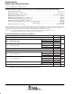
ORDERING INFORMATION
{
T
A
PACKAGE
‡
ORDERABLE
PART NUMBER
TOP-SIDE
MARKING
§
−40°C to 105°C
SOT (SOT-23) − DBV Reel of 3000 SN74AHC1G32TDBVRQ1 A32_
−40°C to 105°C
SOT (SC-70) − DCK Reel of 3000 SN74AHC1G32TDCKRQ1 AG_
†
For the most current package and ordering information, see the Package Option Addendum at the end of
this document, or see the TI web site at http://www.ti.com.
‡
Package drawings, thermal data, and symbolization are available at http://www.ti.com/packaging.
§
The actual top-side marking has one additional character that designates the wafer fab / assembly site.
FUNCTION TABLE
INPUTS
OUTPUT
A B
OUTPUT
Y
H X H
X HH
L L L
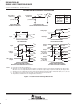
logic diagram (positive logic)
1
2
4
A
B
Y
Copyright 2008, Texas Instruments Incorporated
! "#$ ! %#&'" ($)
(#"! " !%$""! %$ *$ $! $+! !#$!
!(( ,-) (#" %"$!!. ($! $"$!!'- "'#($
$!. '' %$$!)
Please be aware that an important notice concerning availability, standard warranty, and use in critical applications of
Texas Instruments semiconductor products and disclaimers thereto appears at the end of this data sheet.
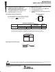
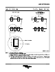
DBV OR DCK PACKAGE
(TOP VIEW)
1
2
3
5
4
A
B
GND
V
CC
Y