
Datasheet


SCLS603A − DECEMBER 2004 − REVISED APRIL 2008
1
POST OFFICE BOX 655303 • DALLAS, TEXAS 75265
D Qualified for Automotive Applications
D Operating Range 2-V to 5.5-V V
CC
D Latch-Up Performance Exceeds 250 mA Per
JESD 17
description/ordering information
The SN74AHC541 octal buffer/driver is ideal for
driving bus lines or buffer memory address
registers. This device features inputs and outputs
on opposite sides of the package to facilitate
printed circuit board layout.
The 3-state control gate is a two-input AND gate with active-low inputs so that if either output-enable (OE1
or
OE2
) input is high, all corresponding outputs are in the high-impedance state. The outputs provide noninverted
data when they are not in the high-impedance state.
To ensure the high-impedance state during power up or power down, OE
should be tied to V
CC
through a pullup
resistor; the minimum value of the resistor is determined by the current-sinking capability of the driver.
ORDERING INFORMATION
{
T
A
PACKAGE
‡
ORDERABLE
PART NUMBER
TOP-SIDE
MARKING
−40°C to 125°C
SOIC − DW Tape and reel SN74AHC541QDWRQ1 AHC541Q
−40
°
C to 125
°
C
TSSOP − PW Tape and reel SN74AHC541QPWRQ1 AHC541Q
†
For the most current package and ordering information, see the Package Option Addendum at the end of this
document, or see the TI web site at http://www.ti.com.
‡
Package drawings, thermal data, and symbolization are available at http://www.ti.com/packaging.
FUNCTION TABLE
(each buffer/driver)
INPUTS
OUTPUT
OE1 OE2 A
OUTPUT
Y
L L L L
L LH H
H XX Z
X H X Z
logic diagram (positive logic)
OE1
OE2
To Seven Other Channels
A1
Y1
1
19
218
Copyright 2008, Texas Instruments Incorporated
!"# $ %&'# "$ (&)*%"# +"#',
+&%#$ %! # $('%%"#$ (' #-' #'!$ '."$ $#&!'#$
$#"+"+ /""#0, +&%# (%'$$1 +'$ # '%'$$"*0 %*&+'
#'$#1 "** (""!'#'$,
Please be aware that an important notice concerning availability, standard warranty, and use in critical applications of
Texas Instruments semiconductor products and disclaimers thereto appears at the end of this data sheet.
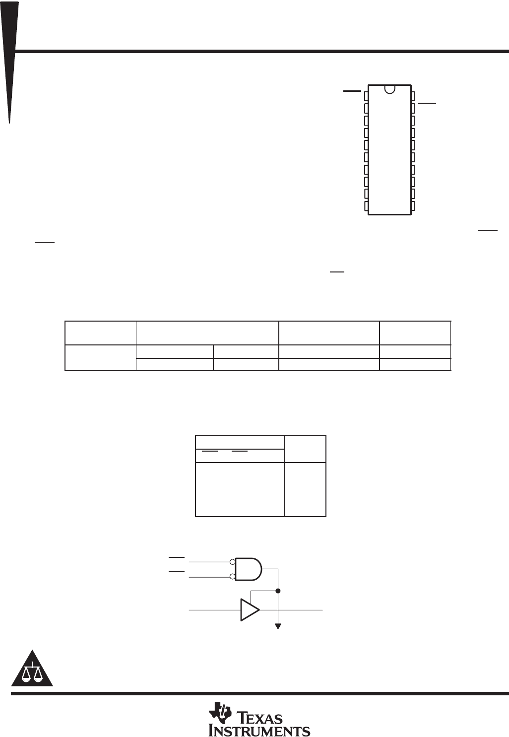
1
2
3
4
5
6
7
8
9
10
20
19
18
17
16
15
14
13
12
11
OE1
A1
A2
A3
A4
A5
A6
A7
A8
GND
V
CC
OE2
Y1
Y2
Y3
Y4
Y5
Y6
Y7
Y8
DW OR PW PACKAGE
(TOP VIEW)